Method of manufacturing a semiconductor device by crystallization of a semiconductor region by use of a continuous wave laser beam through the substrate

a technology of semiconductor devices and crystallization, which is applied in the direction of semiconductor devices, instruments, electrical equipment, etc., can solve the problems of poor crystal quality, difficult uniform irradiation of laser beams, and dislocation in grain boundaries, etc., and achieve the crystallization characteristics of the first semiconductor region.

Inactive Publication Date: 2006-11-07
SEMICON ENERGY LAB CO LTD
View PDF32 Cites 38 Cited by
  • Summary
  • Abstract
  • Description
  • Claims
  • Application Information

AI Technical Summary

Benefits of technology

[0022]In that case, as a method for producing a semiconductor device, an amorphous semiconductor film is formed on a substrate, after adding a catalytic element the amorphous semiconductor film is crystallized by heating treatment to form a crystalline semiconductor film, a first semiconductor region is formed by etching the crystalline semiconductor film, a barrier film covering the first semiconductor region is formed, a heat retaining film covering a top surface and side surfaces of the first semiconductor region is formed through the barrier film, crystalline characteristics of the first semiconductor region are improved by scanning of a continuous wave laser beam from one edge of the first semiconductor region to the other through the substrate, the heat retaining film and the barrier film are removed, and a second semiconductor region is formed by etching the first semiconductor region in a manner that a scanning direction of the laser beam and a channel length direction of a thin film transistor are arranged in almost the same direction.
[0023]As another method for producing a semicon...

Problems solved by technology

However, the crystallization by using a pulsed laser beam can not control a location of nucleation and nucleation density, which causes a spontaneous crystalline nucleus to be expected in the present circumstance.
A created defect and dislocation in not only a grain boundary but also any other locations are caused by shrinkage of a film due to denseness in case of crystallization.
Especially the defect in case of retraction of volume is pointed out that the defect is generated in an outer portion when a semiconductor film divided ...

Method used


Image

  • Method of manufacturing a semiconductor device by crystallization of a semiconductor region by use of a continuous wave laser beam through the substrate
  • Method of manufacturing a semiconductor device by crystallization of a semiconductor region by use of a continuous wave laser beam through the substrate
  • Method of manufacturing a semiconductor device by crystallization of a semiconductor region by use of a continuous wave laser beam through the substrate

Examples


embodiment 1

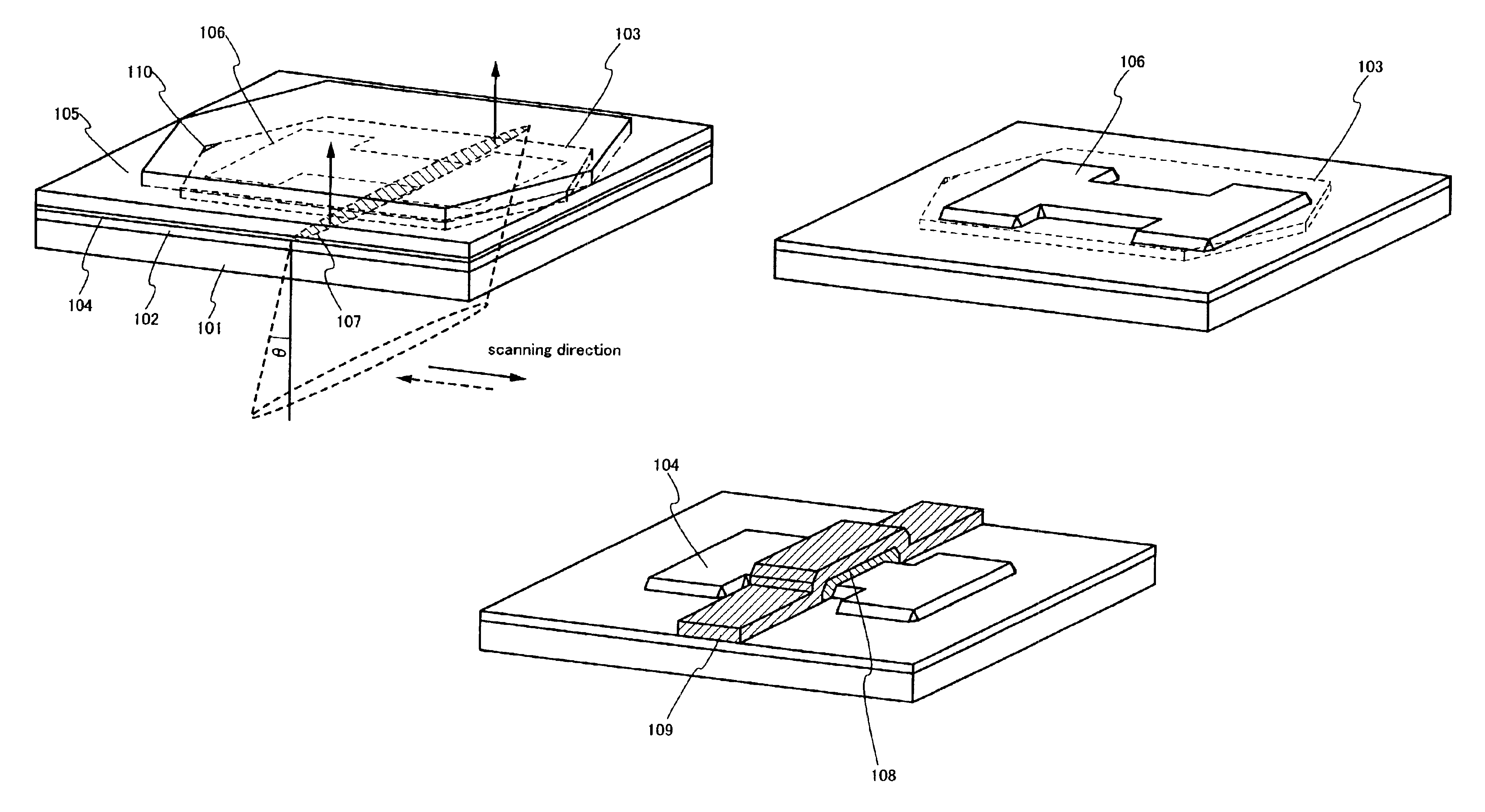
[0102]The embodiment 1 is that fixed resist pattern is formed by photo-engraving in an amorphous silicon film formed on a substrate, a first semiconductor region is formed by etching treatment, a barrier film and a heat retaining film are formed over the first semiconductor region, and the first semiconductor region is crystallized by irradiation of a continuous wave laser beam from the substrate side.

[0103]In FIGS. 10A and 10B, on a glass plate 401 made of aluminosilicate glass, a barrier film 402 is formed of a silicon nitride-oxide film of 100 nm in thickness. A first semiconductor region 403 on the barrier film 402 is a 100 nm thick amorphous silicon film formed by a plasma CVD technique. Top and side surfaces of the first semiconductor region 403 are covered with a 200 nm thick silicon oxide film as a barrier film 404, and the silicon oxide film is covered with a 200 nm thick amorphous silicon film as a heat retaining film 405. FIG. 10A is a top view of the first semiconductor ...

embodiment 2

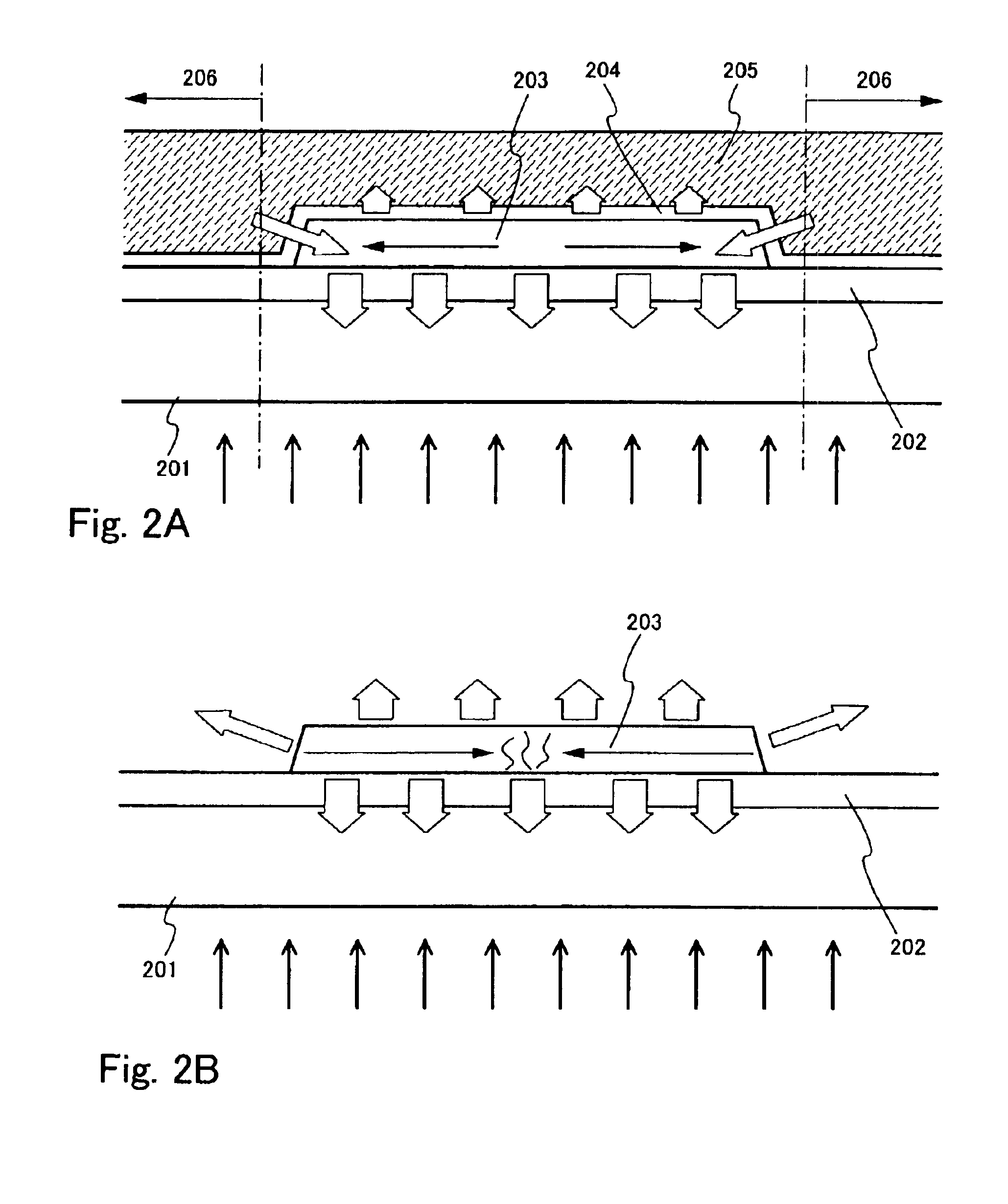
[0114]The scanning of the laser beam in the embodiment 1 may be scanned not only in one direction but also back-and-forth strokes. In this case, the seed regions 406a and 406b may be provided at both sides of the first semiconductor region 403 as shown in the embodiment of FIGS. 13A and 13B. In case of back-and-forth strokes, laser energy density is changed every stroke so that the crystal growth can be phased. The scanning of the laser beam also serves for hydrogen extraction treatment which is often required in case of crystallization of amorphous silicon film. After hydrogen is extracted by scanning at low energy density at first, the crystallization may be performed by the second scanning at higher energy density. This producing method also results in a crystal semiconductor film which crystal grains extend in the scanning direction of the laser beam.

embodiment 3

[0115]The embodiment 3 intends that an amorphous silicon film formed on a substrate is crystallized in advance and enlargement of a crystal grain by a continuous wave laser beam.

[0116]As shown in FIG. 15A, blocking layer 502 and a amorphous silicon film 503 are formed on a glass substrate 501 like the embodiment 1. A 100 nm thick oxide silicon film as a masking insulation film 504 is formed on the blocking layer 502 and the amorphous silicon film 503 by plasma CVD technique, and an opening 505 is provided. In order to add Ni as a catalytic element, water solution containing 5 ppm nickel acetate is spin-coated. Ni is in contact with the amorphous silicon film at the opening 505. A location where the opening 505 is formed is located in the seed region of the first semiconductor region which is formed later or out side of the seed region.

[0117]Then, as shown in FIG. 15B, the amorphous silicon film is crystallized by a 4 hours heat treatment at a temperature of 580° C. The crystallizati...


PUM


Abstract

A technique is provided for forming a crystalline semiconductor film whose orientation is uniform by control of crystal orientation and obtaining a crystalline semiconductor film in which concentration of an impurity is reduced. A configuration of the invention is that a first semiconductor region is formed on a substrate having transparent characteristics of a visible light region, a barrier film is formed over the first semiconductor region, a heat retaining film covering a top and side surfaces of the first semiconductor region is formed over the barrier film, the first semiconductor region is crystallized by scanning a continuous wave laser beam from one edge of the first semiconductor region to the other through the substrate, then the heat retaining film and the barrier film are removed and a second semiconductor region is formed as an active layer of TFT by etching the crystallized first semiconductor region. A pattern of the second semiconductor region formed by etching is formed in a manner that a scanning direction of the laser beam and a channel length direction of the TFT are arranged in almost the same direction in order to smooth drift of carriers.

Description

BACKGROUND OF THE INVENTION[0001]1. Field of the Invention[0002]The present invention relates to a method for producing a semiconductor device by employing a laser annealing method. More particularly, the invention relates to a technique for improving crystallization of an amorphous semiconductor film or crystalline characteristics by a laser beam.[0003]2. Description of the Related Art[0004]A technique, which an amorphous semiconductor film formed on a substrate such as a glass is crystallized by a laser annealing method, has been developed. The laser annealing method described in the specification includes a technique re-crystallizing a damaged layer or an amorphous layer which is formed in a semiconductor substrate or a semiconductor film, a technique crystallizing an amorphous semiconductor film formed on a substrate, or a technique improving crystalline characteristics of a semiconductor film (crystalline semiconductor film) having a crystal structure. In a laser oscillation ma...

Claims


Application Information

Patent Timeline
IPC IPC(8): H01L21/26H01L21/324H01L21/42H01L21/477H01L21/20G02F1/13H01L21/268H01L21/322H01L21/336H01L21/77H01L21/84H01L27/12H01L29/786
CPCH01L21/2026H01L21/268H01L21/3221H01L27/12H01L29/66757H01L29/78621H01L29/78675H01L29/78684H01L27/1281H01L27/1285H01L21/02683H01L21/02678H01L21/02488H01L21/02422H01L21/02532H01L21/02609H01L21/0242H01L21/02672H01L21/02691G02F1/13
Inventor YAMAZAKI, SHUNPEI
Owner SEMICON ENERGY LAB CO LTD
Why Eureka
Try Eureka