

Modulating etch selectivity and etch rate of silicon nitride thin films
a technology of etch selectivity and etch rate, which is applied in the direction of electrical equipment, decorative surface effects, decorative arts, etc., can solve the problems of undesirable etching of the underlying film, unsatisfactory etching of the other film,
- Summary
- Abstract
- Description
- Claims
- Application Information
AI Technical Summary
Benefits of technology
Problems solved by technology
Method used
Image

Examples
Embodiment Construction
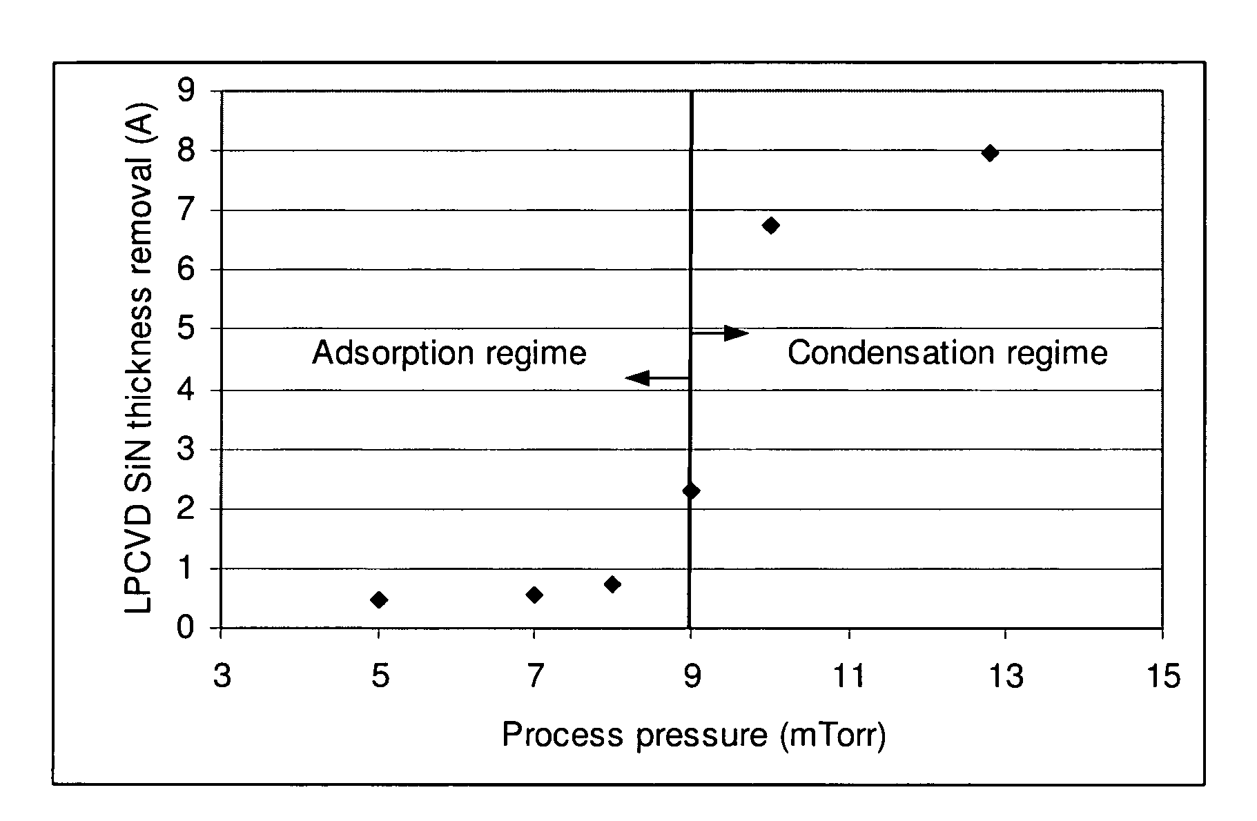
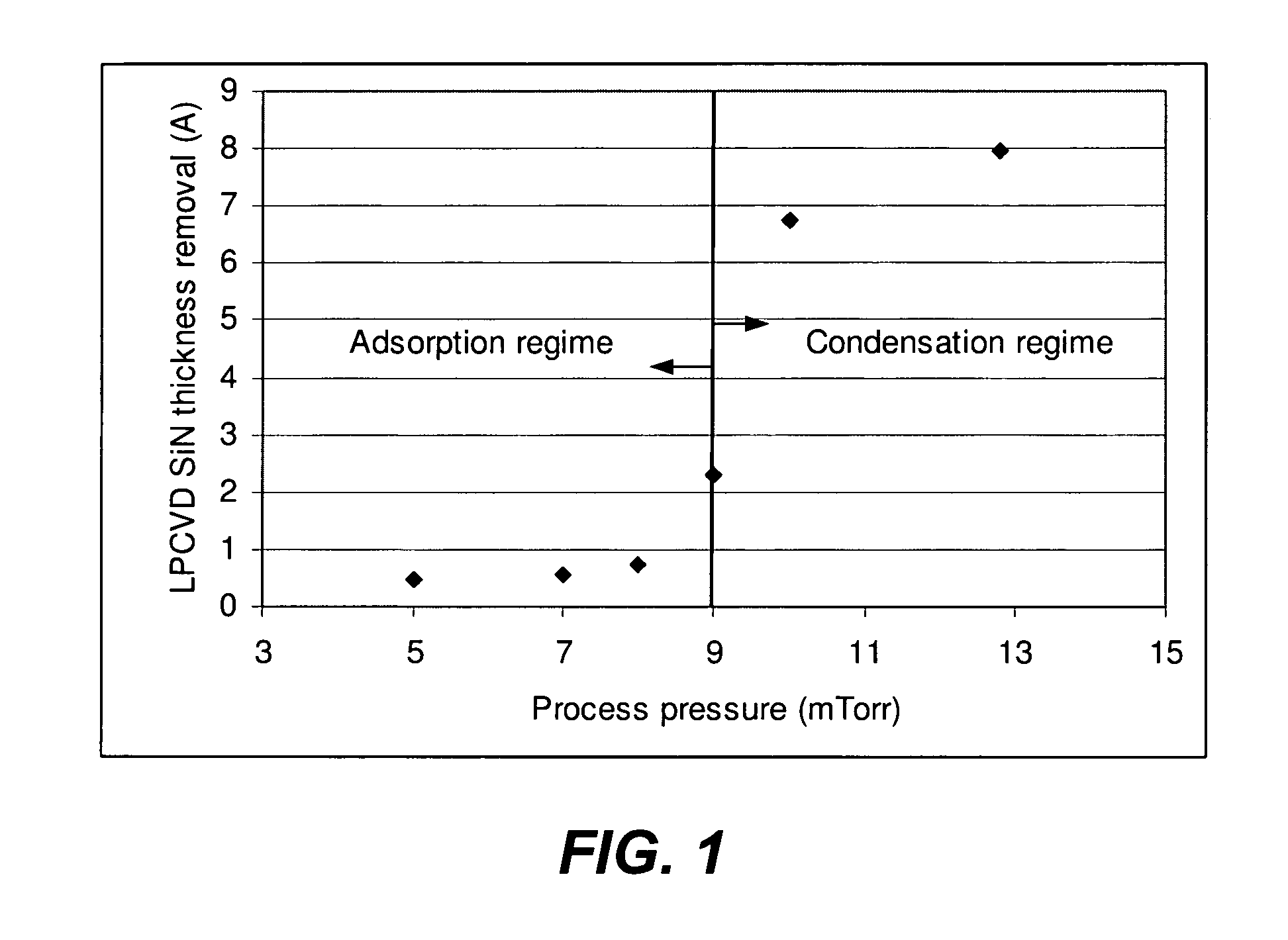
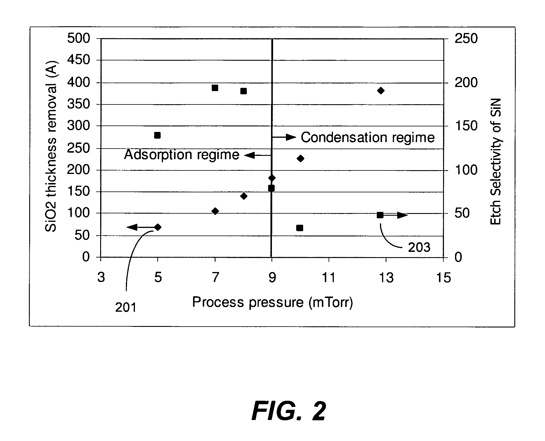
[0029]Aspects of the present invention are directed to etching of materials from substrates using an atomic layer removal (ALR™) process, such as partially fabricated integrated circuits. While the methods of present invention find particular use in the processing of semiconductor substrates, they can also be employed in other applications, such as removal of oxide material from other workpieces such as those employed in flat panel display manufacturing.
Fluorine and Hydrogen Gas Based Selective Etching
[0030]The fluorine- and hydrogen-containing gas based selective etching of silicon oxide is a two-step process. The first step is the etching of silicon oxide by exposing the silicon oxide surface to fluorine- and hydrogen-containing species, or alternatively, to other precursors that would form the ammonium fluoride or ammonium bifluoride etchant, or directly to the etchants. The hydrogen-containing reactant may include one or more of ammonia (NH3), hydrogen (H2) or water vapor (H2O)....
PUM
| Property | Measurement | Unit |
|---|---|---|
| pressure | aaaaa | aaaaa |
| pressure | aaaaa | aaaaa |
| pressure | aaaaa | aaaaa |
Abstract
Description
Claims
Application Information