Substrate processing method and method of manufacturing crystalline silicon carbide (SIC) substrate

a technology of crystalline silicon carbide and substrate, which is applied in the direction of basic electric elements, electrical apparatus, semiconductor devices, etc., can solve the problems of increasing the number of processes, difficulty in ensuring the reproducibility of maintaining the surface flatness of silicon carbide samples, and the concern of heavy metal contamination of resists, so as to reduce surface roughness

Active Publication Date: 2012-05-29
CANON ANELVA CORP
View PDF13 Cites 4 Cited by
  • Summary
  • Abstract
  • Description
  • Claims
  • Application Information

AI Technical Summary

Benefits of technology

[0011]The technology disclosed in patent document 2 is an effective technology in that the partial pressure of the remaining water under an annealing atmosphere is controlled during the annealing and thus it is possible to reduce the surface roughness (RMS value) of the substrate, that is, the surface flatness of silicon carbide (SiC); the technology sufficiently achieved electrical activation required in those times. However, in consideration of enhancement of yield and the like, it is desirable to achieve further enhanced surface flatness.
[0015]Therefore, in patent document 3, it is necessary to form the ion implantation region thicker than the thickness of the necessary ion implantation region, by a thickness corresponding to a portion removed by the plasma etching. In other words, it is necessary to form the ion implantation region that has not only an originally required amount (thickness) but also an extra thickness; in consideration of cost and yield, it is required to achieve the flatness of the surface of the single crystal silicon carbide (SiC) substrate while reducing the amounts of epitaxial layer and impurity used for formation of the extra ion implantation region.
[0016]The present invention is made in view of the foregoing problem; an object of the present invention is to provide a method of processing a substrate in which, when a crystalline silicon carbide (SiC) substrate is subjected to annealing processing, the occurrence of the surface roughness is suppressed and a method of manufacturing the silicon carbide (SiC) substrate.
[0021]According to the substrate processing method and the method of manufacturing the crystalline silicon carbide (SiC) substrate of the present invention, when the high temperature heating processing (for example, annealing processing) is performed on the crystalline silicon carbide (SiC) substrate, it is possible to reduce the surface roughness on the crystalline silicon carbide (SiC) substrate on which the high temperature heating processing is performed.

Problems solved by technology

However, in the substrate heat treatment device and the heat treatment method described in non-patent document 1, since it is very difficult to control additive amount of silane (SiH4) gas, there is such a problem that a droplet (liquefied and aggregated silicon) of silicon (Si) may occur, or that the change in the amount of water brought from the substrate makes it difficult to ensure reproducibility of maintaining surface flatness of a silicon carbide (SiC) sample after activation annealing.
In the substrate heat treatment device disclosed in patent document 1, since a substrate to be processed is coated with a resist and is carbonized in a special high-temperature furnace, and thus the substrate to be processed is carbon-coated, the number of processes is increased, and there is a concern of contamination by heavy metals from the resist.
In the substrate heat treatment method disclosed in patent document 2, when aluminum (Al) is implanted as an impurity, a very high temperature of about 1900° C. is required to achieve an activation rate of 100%; in this case, step bunching is not observed but holes such as pits may be locally produced, and this may cause a leak in a pn junction.

Method used


Image

  • Substrate processing method and method of manufacturing crystalline silicon carbide (SIC) substrate
  • Substrate processing method and method of manufacturing crystalline silicon carbide (SIC) substrate
  • Substrate processing method and method of manufacturing crystalline silicon carbide (SIC) substrate

Examples


example 1

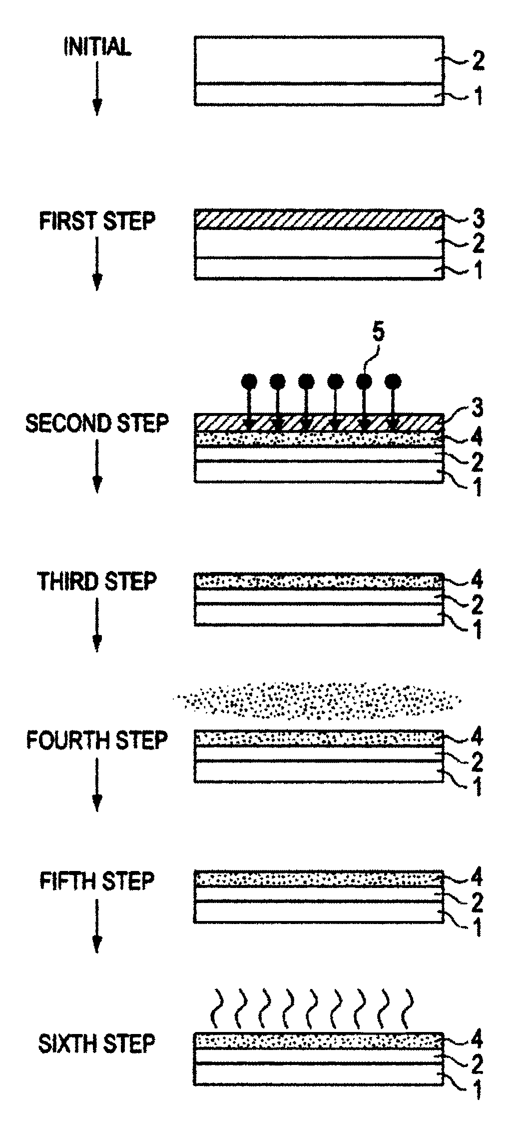
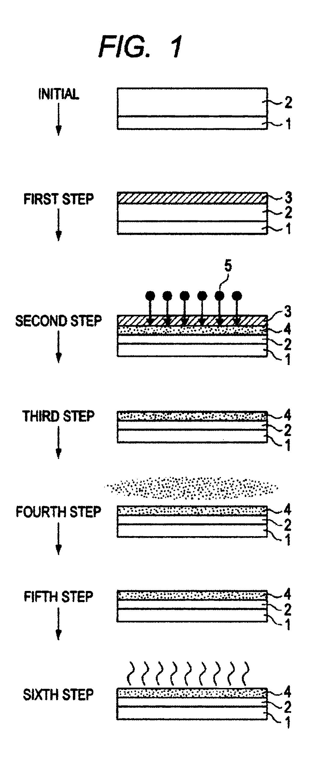
[0048]By the substrate processing method 1, the substrate processing method of the single crystal silicon carbide (SiC) substrate was performed. The plasma irradiation by the inductively coupled plasma (ICP) etcher in the fourth step was performed using a mixed gas of argon (Ar) gas and carbon tetrafluoride (CF4) gas under conditions shown in table 1.

[0049]

TABLE 1RF power of an upper coil400WSubstrate bias150WCF4 gas flow rate30sccmAr gas flow rate20sccmEtching pressure0.2PaPlasma irradiation period10secondsSiC etching amount20nm

[0050]In the high temperature heating processing in the fifth step, the activation annealing processing was performed using a high-frequency induction heating furnace at a temperature of 1700° C. for ten minutes.

[0051]The surface roughness (RMS value: root mean square value) of the obtained substrate was measured using an atomic force microscope (AFM: atomic force microscopy). The measurement was performed in a damping force mode over a measurement area of 4...

example 2

[0060]In order to reduce the amount of etching of the silicon carbide (SiC) substrate by the plasma irradiation, the substrate processing was performed under conditions shown in table 2, instead of using the plasma conditions of the inductively coupled plasma (ICP) etcher in the fourth step in example 1.

[0061]

TABLE 2RF power of the upper coil400WSubstrate bias0WCF4 gas flow rate30sccmAr gas flow rate20sccmEtching pressure0.2PaPlasma irradiation period60secondsSiC etching amount0nm

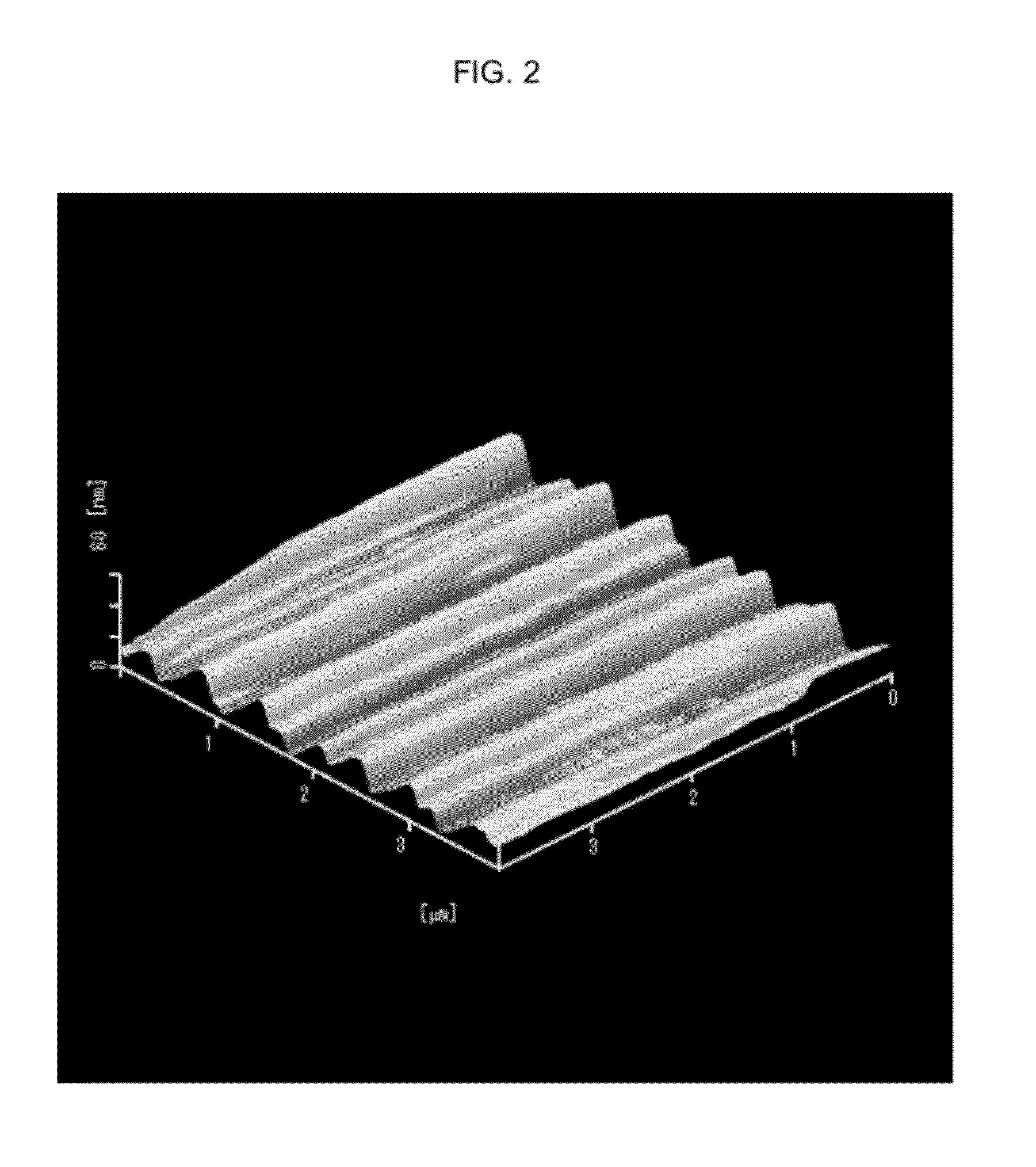
[0062]FIG. 5 is a surface observation diagram after annealing processing in the present example. When the surface roughness was observed by AFM, the RMS value was 1.6 nm; it has been found that the preprocessing by the plasma irradiation before the annealing process has the effect of reduction in the surface roughness when the high temperature processing is performed on the single crystal silicon carbide (SiC) (FIG. 5).

[0063]As described above, in the present example, it has been found from table 2 and FIG....

example 3

[0064]In order to evaluate the flow rate ratio of a process gas by the plasma irradiation, the substrate processing was performed under conditions shown in table 3, instead of using the plasma irradiation conditions by the inductively coupled plasma (ICP) etcher in the fourth step in example 1.

[0065]

TABLE 3RF power of the upper coil400WSubstrate bias0WCF4 gas flow rate0sccmAr gas flow rate20sccmEtching pressure0.2PaPlasma irradiation period60secondsSiC etching amount0nm

[0066]FIG. 6 is a surface observation diagram after annealing processing in the present example. When the surface roughness was observed by AFM, the RMS value was 2.1 nm; it has been found that, although the preprocessing by the plasma irradiation before the annealing processing with only the argon (Ar) gas has a small effect as compared with the case where the carbon tetrafluoride (CF4) gas was added, the preprocessing has the effect of reduction in the surface roughness when the high temperature processing is perfor...


PUM

PropertyMeasurementUnit
temperatureaaaaaaaaaa
thicknessaaaaaaaaaa
thicknessaaaaaaaaaa

Abstract

The present invention provides a method of processing a substrate and a method of manufacturing a silicon carbide (SiC) substrate in which, when annealing processing is performed on a crystalline silicon carbide (SiC) substrate, the occurrence of surface roughness is suppressed. A substrate processing method according to an embodiment of the present invention includes a step of performing plasma irradiation on a single crystal silicon carbide (SiC) substrate (1) and a step of performing high temperature heating processing on the single crystal silicon carbide (SiC) substrate (1) in which the plasma irradiation is performed.

Description

CROSS-REFERENCES TO RELATED APPLICATIONS[0001]This application is a continuation application of International Application No. PCT / JP2010 / 054437, filed Mar. 16, 2010, which claims the benefit of Japanese Patent Application No. 2009-076313, filed Mar. 26, 2009. The contents of the aforementioned applications are incorporated herein by reference in their entities.TECHNICAL FIELD[0002]The present invention relates to a method of preprocessing a crystalline silicon carbide (SiC) substrate such as of single crystal silicon carbide (SiC) and a method of manufacturing the crystalline silicon carbide (SiC) substrate. More particularly, the present invention relates to a technology for acquiring surface flatness by preprocessing in a method of heat-treating the substrate.BACKGROUND ART[0003]In order to electrically activate an impurity implanted into a single crystal silicon carbide (SiC) substrate, an activation annealing processing process is performed at a high temperature. However, when t...

Claims


Application Information

Patent Timeline
Patent Type & Authority Patents(United States)
IPC IPC(8): H01L21/265
CPCH01L21/0445H01L21/324Y10S438/931H01L21/3247
Inventor SHIBAGAKI, MASAMISATOH, MASATAKASATOH, LEGAL REPRESENTATIVE, AKEMISUGIMOTO, TAKAHIRO
Owner CANON ANELVA CORP
Why Eureka
Try Eureka