Multiplexed output two terminal photodiode array for imaging applications and related fabrication process

a photodiode array and multi-pixel technology, applied in the field of imaging systems, can solve the problems of limiting the dynamic range and/or sensitivity, significantly reducing the area occupancy ratio between the sensing area and the overall chip area (geometrical fill factor), and affecting the integration of the detector with the ancillary electronics.

Active Publication Date: 2012-09-11
STMICROELECTRONICS SRL
View PDF5 Cites 9 Cited by
  • Summary
  • Abstract
  • Description
  • Claims
  • Application Information

AI Technical Summary

Benefits of technology

[0019]The effectiveness of such a modulation of these fundamentally geometric parameters in determining the resulting depth of the profile (thickness) of the depletion layer (i.e. of the sensible photon absorption region in the semiconductor) and the pinch-off condition of depletion regions produced around the uniformly spaced Schottky metal / semiconductor trench contacts of the each pixel photodiode (i.e. corresponding to its maximum detection efficiency condition) has been found to be substantially equivalent for a variety of commonly used semiconductors. By properly designing the geometrical aspect ratio and spacing of the metal filled trenches, it may be retained also at very low reverse bias condition of the diodes and even at null bias, that is under purely photovoltaic regime.
[0021]It may be well known that in any semiconductor material the photon absorption coefficient decreases with the wavelength (See, for example, H. Y. Cha and P. M. Sandvik, Electrical and Optical Modeling of 4H—SiC Avalanche Photodiodes, Japanese Journal of Applied Physics, Vol. 47, No. 7, pp. 5423-5425, 2008, and S. M. Sze, Semiconductor Devices Physics and Technology, New York: Wiley, 1985). At 350 nm, for instance, the “absorption length” in 4H—SiC is about 35 μm, meaning that 67% of the incident optical flux at this wavelength is absorbed in an active layer (a depleted semiconductor region) 35 μm thick (See J. Hu et al., 4H—SiC Visible-Blind Single-Photon Avalanche Diode for Ultraviolet Detection at 280 and 350 nm, IEEE Transactions on Electron Devices, Vol. 55, No. 8, pp. 1977-1982, 2008). This means that it may be generally necessary to increase as much as required or possible, the thickness of the active region (i.e. the depth of the depleted region in the semiconductor) to enhance absorption, and consequently, photon detection effectiveness at the long wavelength end of the sensitivity range of the semiconductor. The ability to grow lightly doped semiconductor epilayers of low defectivity and of relatively large thickness, in the order of several tens of μm, and the ability to etch deep trenches with a high aspect ratio in a semiconductor epilayer and to fill them with a high Schottky barrier metal, may make it relatively easy to adapt the geometric parameters that determine the operative thickness (depth) of the depletion layer amongst the Schottky photodiode structures of individual array pixels (i.e. designing the geometry of the photodiode of each pixel for a unique response to illumination with photons of a given wavelength).
[0022]A relatively light doping of a semiconductor epilayer, in which the array of Schottky photodiodes is formed, may promote the creation of wide depleted regions already at very low reverse bias condition of the diodes. By suitably designing the distance among adjacent trenches, the pinch-off condition, corresponding to the condition of fullest detection effectiveness, may be achieved with a relatively low reverse bias and may be even in photovoltaic regime (0 V bias of the photodiode).

Problems solved by technology

The packaging of these devices and the integration of the detector with the ancillary electronics is a quite complex matter, and lately various techniques have been developed to realize compact and cheap “packaging” approaches.
In case of a multi-pixel array, an individual connection of each array pixel to an external circuitry may be desired, and for arrays with a large number of pixels wire bonding may become practically impossible because of packaging constraints.
However, this approach significantly reduces the area occupancy ratio between sensing area and overall chip area (geometrical fill factor) limiting the dynamic range and / or sensitivity (See Niclass et al., Design and Characterization of a CMOS 3-D Image Sensor Based on Single Photon Avalanche Diodes, IEEE Journal of Solid-State Circuits, Vol. 40, No. 9, pp.
Moreover, it may not be possible to integrate the electronics and the photo sensor fabrication technologies in a monolithic device fabrication process.
Moreover because of the vias, most of the required photolithographic steps are done on a non-planar surface, which raises some problems of non-uniform photo resist thickness and exposure depth-of-focus issues.
However, high cost of these techniques make them unsuited for low-end products (See K. Takahashi and M. Sekiguchi, Through Silicon Via and 3-D Wafer / Chip Stacking Technology, 2006 Symposium on VLSI Circuits, pp.

Method used


Image

  • Multiplexed output two terminal photodiode array for imaging applications and related fabrication process
  • Multiplexed output two terminal photodiode array for imaging applications and related fabrication process
  • Multiplexed output two terminal photodiode array for imaging applications and related fabrication process

Examples


Embodiment Construction

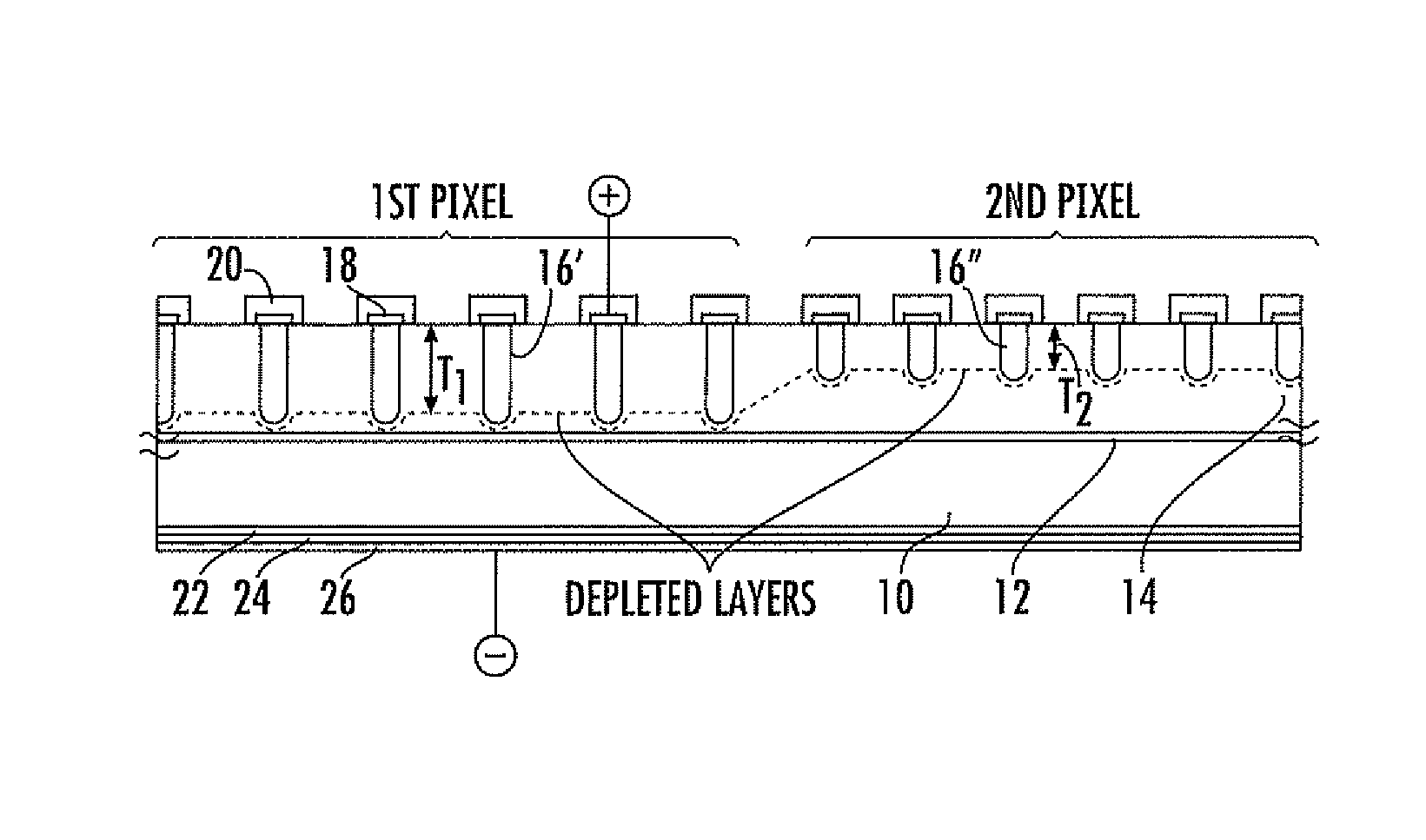
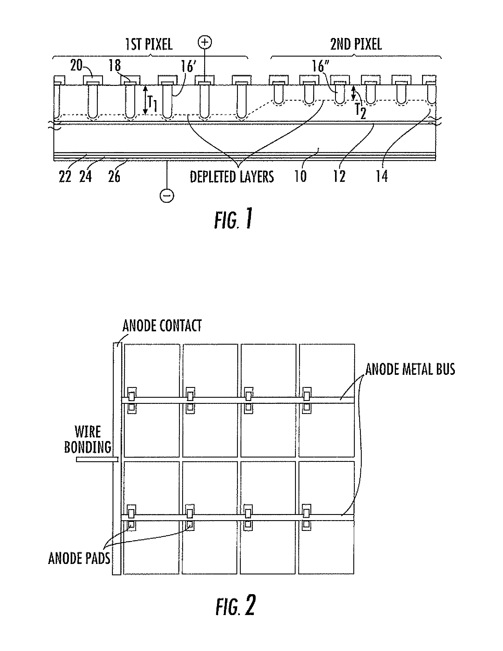
[0027]The novel architecture of multi-pixel photo detector array of Schottky photodiodes for imaging applications with substantially monochromatic radiations of wavelength comprised in a high wavelength end portion of the sensitivity range of the semiconductor used is schematically depicted in FIG. 1.

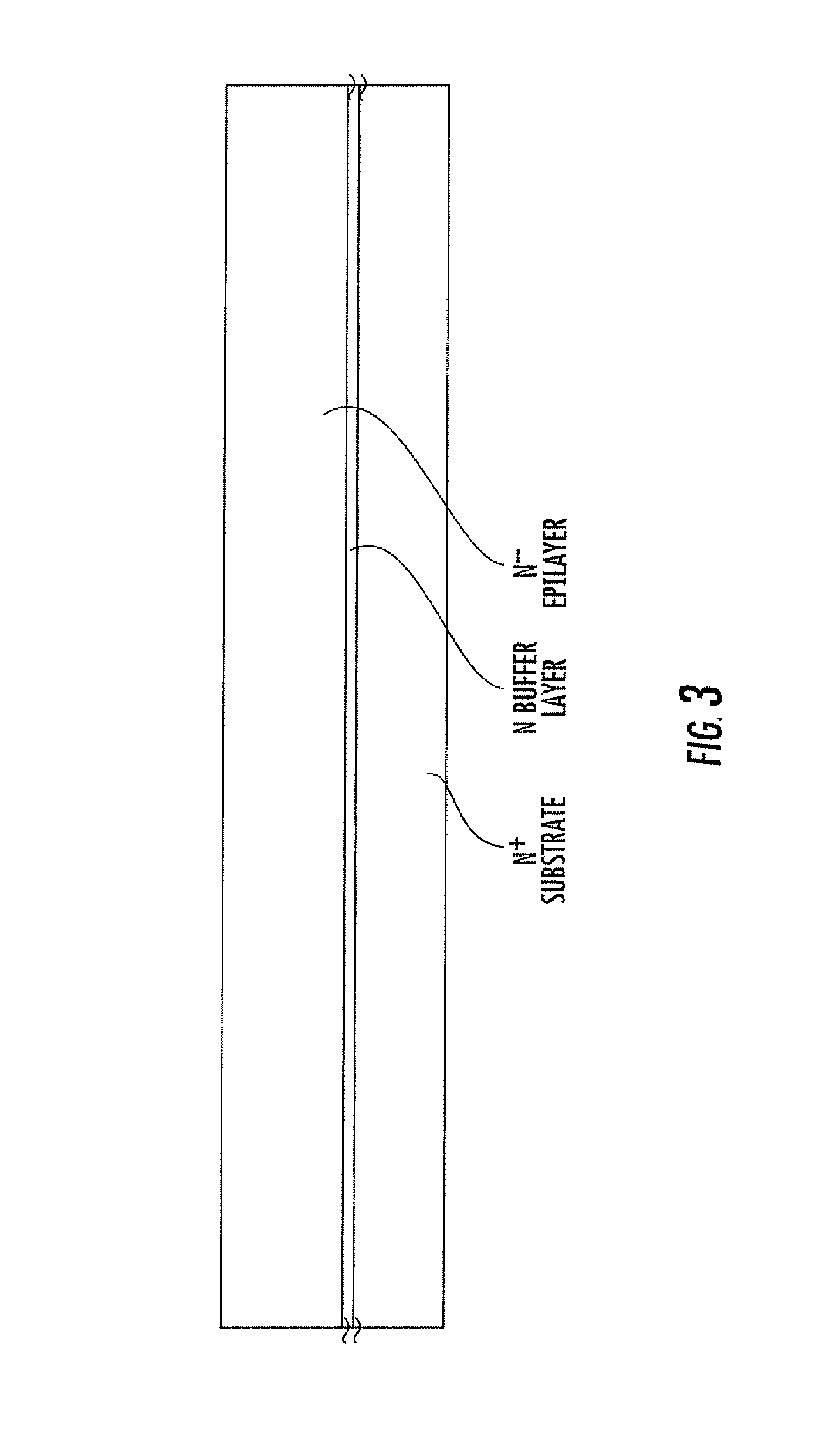
[0028]According to the considered exemplary embodiment, FIG. 1 shows a vertical cross-sectional view of two adjacent pixels of the array. Alike are the two pixels, 1ST—PIXEL and 2ND—PIXEL, shown in the descriptive fragment of the cross-sectional view of FIG. 1. The pixel photodiodes are formed in a lightly doped, n−− type layer 14, epitaxially grown over a relatively thin moderately doped, n− type buffer layer 12, on a heavily doped, n+ type mono crystalline substrate 10. The cathode contact-terminal pad of the array is common to all the pixels and may be formed by a commonly, not patterned, metal layer or, more typically, a multilayer metal stack, 22, 24 and 26, deposited over the rear...


PUM


Abstract

A detector array for an imaging system may exploit the different sensitivities of array pixels to an incident flux of low energy photons with a wavelength falling near the high end of the range of sensitivity of the semiconductor. The detector array may provide the de-multiplexable spatial information. The detector array may include a two-terminal multi-pixel array of Schottky photodiodes electrically connected in parallel.

Description

FIELD OF THE INVENTION[0001]The invention relates generally to imaging systems. In particular, the invention relates to a multi-pixel detector array for use in an imaging system and a method of fabricating the same.BACKGROUND OF THE INVENTION[0002]Detector arrays are used in a wide variety of imaging systems for industrial as well as scientific applications. For example, detector arrays have been recently widely used in nuclear medical imaging techniques, such as Positron Emission Tomography (PET). In such an application 511 keV gamma rays emitted from a human body strike pixelated scintillators which create light in response to the received radiation. Each illuminated pixel of the pixelated scintillator is detected by a respective photodiode of the detector array that converts the light into electrical signals used for imaging purposes. During data collection, each pixel provides an electrical output signal proportional to the absorbed photon flux. These output signals are then pro...

Claims


Application Information

Patent Timeline
Patent Type & Authority Patents(United States)
IPC IPC(8): H01L21/02
CPCH01L27/14643H01L31/085H01L31/108
Inventor MAZZILLO, MASSIMO CATALDO
Owner STMICROELECTRONICS SRL
Why Eureka
Try Eureka