
High voltage MOSFET diode reverse recovery by minimizing P-body charges

a technology of mosfet diodes and reverse recovery, which is applied in the direction of diodes, semiconductor devices, electrical apparatus, etc., can solve the problems of large turn off time and loss, igbt devices implemented for power supply and motor control applications often suffer from limitations of high qrr and power loss, and adversely affect production costs

Active Publication Date: 2012-12-04
ALPHA & OMEGA SEMICON INC
View PDF1 Cites 10 Cited by
  • Summary
  • Abstract
  • Description
  • Claims
  • Application Information

AI Technical Summary

Benefits of technology

"The present invention provides a new and improved method and device configuration for manufacturing a semiconductor power device that integrates a Schottky diode with a semiconductor power device without requiring an additional mask. This method reduces the distance between the edge of the planar gates to the field oxide to form self-aligned body regions, resulting in a more softness factor and reduced Qrr, Trr, and increasing the softness factor S. Additionally, the method reduces the amount of body-type charges available for high level injections, further improving the device's performance. The semiconductor power device includes a semiconductor substrate with an active cell area and a termination area, and the device configuration includes a patterned Schottky metal layer covering a portion of the active cell area and a patterned field oxide layer in the termination area. The method includes steps of growing and patterning a field oxide layer in the termination area and also in the active cell area, depositing and patterning a polysilicon layer, and performing a blank body dopant implant to form body dopant regions. The semiconductor power device can also include high concentration body-dopant regions and an insulated gate bipolar transistor power device."

Problems solved by technology

A high level injection into the N− Epi region from the P-body regions causes a large turn off time and losses.
A high voltage MOSFET, a super-junction semiconductor power device, and IGBT devices when implemented for the power supply and motor control applications often suffer from the limitations of high Qrr and power loss.
However, conventional configurations and methods of manufacturing the semiconductor power devices usually require an additional mask to block an area in order to integrate the Schottky diode as an internal diode of the power device in that area.
Production costs are adversely affected due to additional this mask requirement.

Method used


Image

  • High voltage MOSFET diode reverse recovery by minimizing P-body charges
  • High voltage MOSFET diode reverse recovery by minimizing P-body charges
  • High voltage MOSFET diode reverse recovery by minimizing P-body charges

Examples


Embodiment Construction

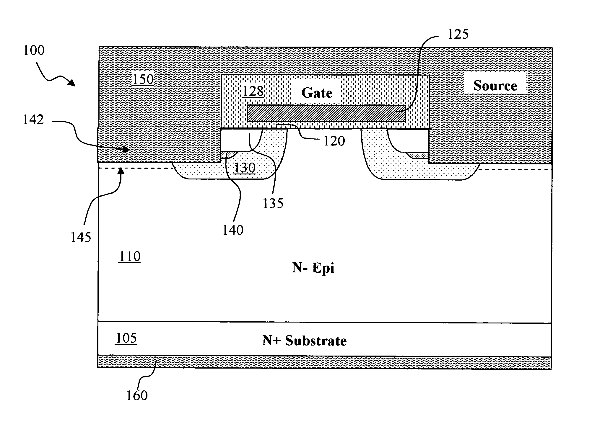
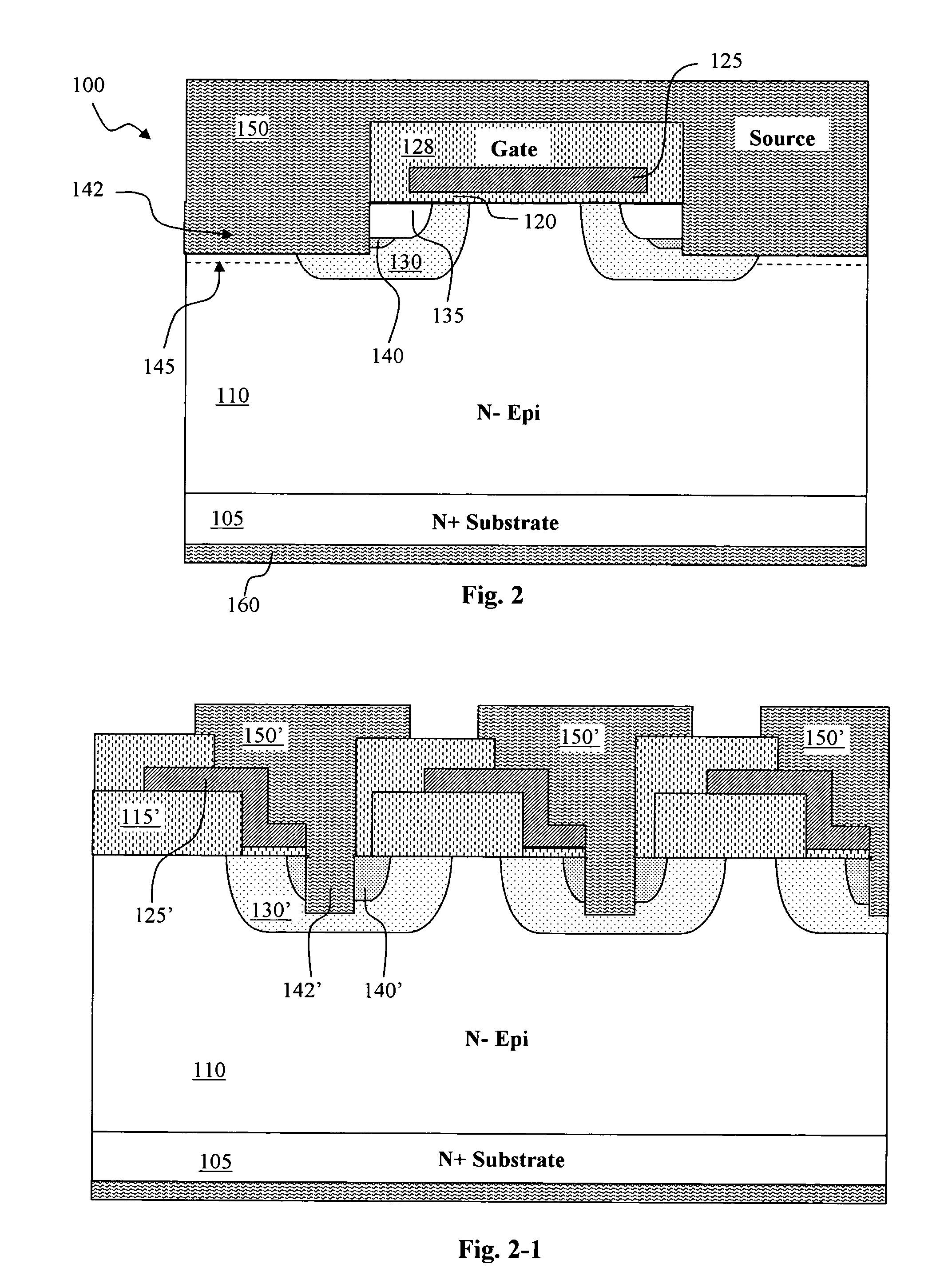
[0028]Referring to FIG. 2 for a cross sectional view of active cell 100 of a high voltage MOSFET (HV MOSFET) semiconductor power device of this invention. The HV MOSFET device is supported on an N+ silicon substrate 105 with an epitaxial layer 110 formed on top of the N+ substrate 105. A planar gate 125 is formed on top of a gate oxide layer 120. A P-body region 130 is formed in the epitaxial layer below the gate oxide layer 120 encompassing an N+ source region 135. The MOSFET device 100 further includes a P+ doped region 140 within the P-body region 130. A source metal 150 covering the top surface with direct contact to the source region 135 and the P-body region 130. A drain metal 160 to function as a drain electrode is formed on the back side of the semiconductor substrate 105 thus forming an active cell of vertical MOSFET power device. The drawing is not to scale, as the substrate 105 is typically several times thicker than the epitaxial layer 110. A contact trench 142 is formed...


PUM


Abstract

This invention discloses a method for manufacturing a semiconductor power device in a semiconductor substrate comprises an active cell area and a termination area. The method comprises the steps of a) growing and patterning a field oxide layer in the termination area and also in the active cell area on a top surface of the semiconductor substrate b) depositing and patterning a polysilicon layer on the top surface of the semiconductor substrate at a gap distance away from the field oxide layer; c) performing a blank body dopant implant to form body dopant regions in the semiconductor substrate substantially aligned with the gap area followed by diffusing the body dopant regions into body regions in the semiconductor substrate; d) implanting high concentration body-dopant regions encompassed in and having a higher dopant concentration than the body regions e) applying a source mask to implant source regions having a conductivity opposite to the body region with the source regions encompassed in the body regions and surrounded by the high concentration body-dopant regions; and f) etching contact trenches into the source, body contact, and body regions.

Description

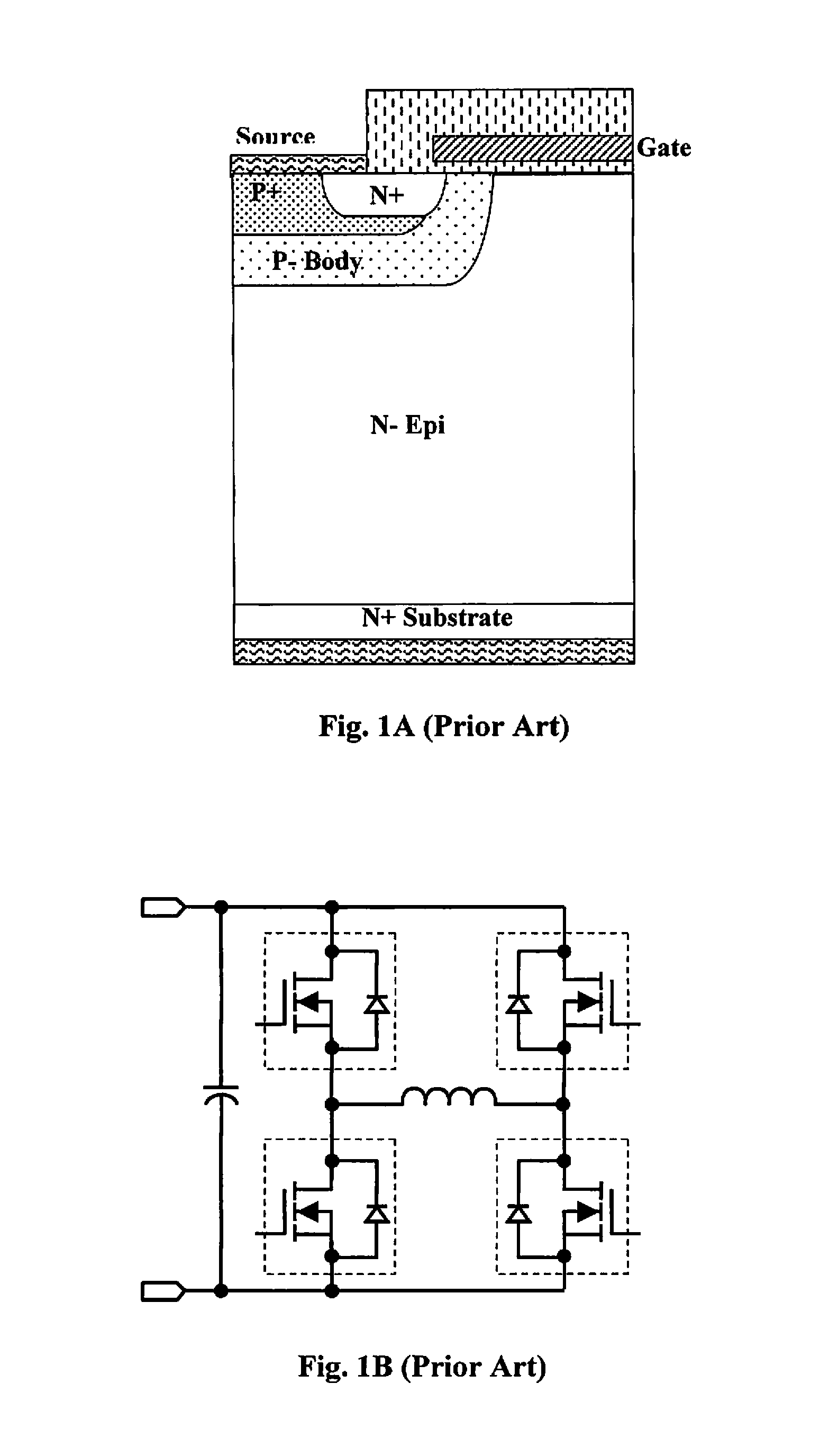
BACKGROUND OF THE INVENTION[0001]1. Field of the Invention[0002]The invention relates generally to the configurations and methods of manufacturing semiconductor power devices. More particularly, this invention relates to a device configuration and method of manufacturing semiconductor power devices integrated with Schottky diode without requiring additional masks, for reducing the turn off time and the power losses.[0003]2. Description of the Prior Art[0004]There is a great demand for implementing a semiconductor power device by integrating the Schottky diode as an internal diode. Specifically, the high voltage metal oxide semiconductor field effect transistor (HV MOSFET) behaves like a P-i-N diode with a negative drain-to-source voltage Vds<0, due to the built-in body diode formed by the P+, P− Body, and N-epi as shown in FIG. 1A. A high level injection into the N− Epi region from the P-body regions causes a large turn off time and losses. Furthermore, a high rate of current var...

Claims


Application Information

Patent Timeline
Patent Type & Authority Patents(United States)
IPC IPC(8): H01L29/739H01L21/336H01L29/78H01L21/331
CPCH01L29/7806H01L29/7811H01L29/0634H01L29/41766H01L29/66727H01L29/7396H01L29/7805H01L29/0619H01L29/0696H01L29/1095H01L29/404
Inventor BOBDE, MADHURGUAN, LINGPENGBHALLA, ANUP
Owner ALPHA & OMEGA SEMICON INC
Learn More