Supercharge Your Innovation With Domain-Expert AI Agents!

Mask blank and method of manufacturing mask

a mask and mask technology, applied in the field of mask blanks and mask manufacturing methods, can solve the problems that the cd uniformity or cd linearity of the mask required in the next-generation semiconductor design rule (32 nm) cannot be achieved, and achieve the effect of excellent cd uniformity and cd linearity

Active Publication Date: 2013-02-05
HOYA CORP +1
View PDF21 Cites 0 Cited by
  • Summary
  • Abstract
  • Description
  • Claims
  • Application Information

AI Technical Summary

Benefits of technology

The invention aims to provide a mask blank that can be used to make a mask with good CD uniformity and linearity. The mask blank includes a hard mask that satisfies requirements for conductivity, etching selectivity, and a chromium light-shielding film. The use of this mask blank results in a mask with excellent performance.

Problems solved by technology

However, according to the study by the present inventor, it has been found that the technique described in Patent Document 2 has the following problem.
That is, because of the increase in FC correction amount, there is a problem that the CD uniformity or the CD linearity of a mask required in the next-generation semiconductor design rule (after DRAM half-pitch 32 nm) cannot be achieved.

Method used


Image

  • Mask blank and method of manufacturing mask
  • Mask blank and method of manufacturing mask
  • Mask blank and method of manufacturing mask

Examples


first embodiment

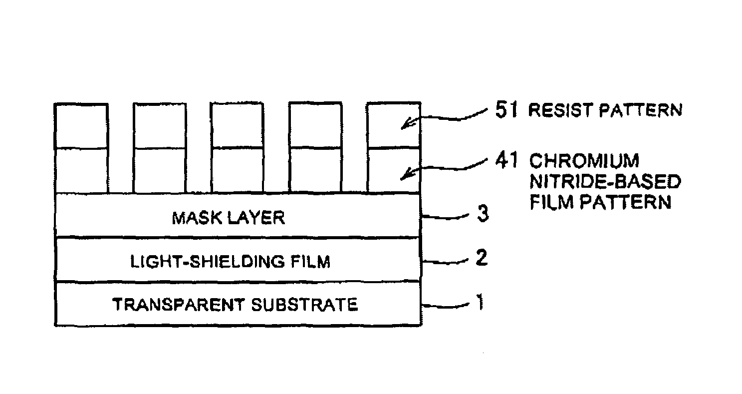
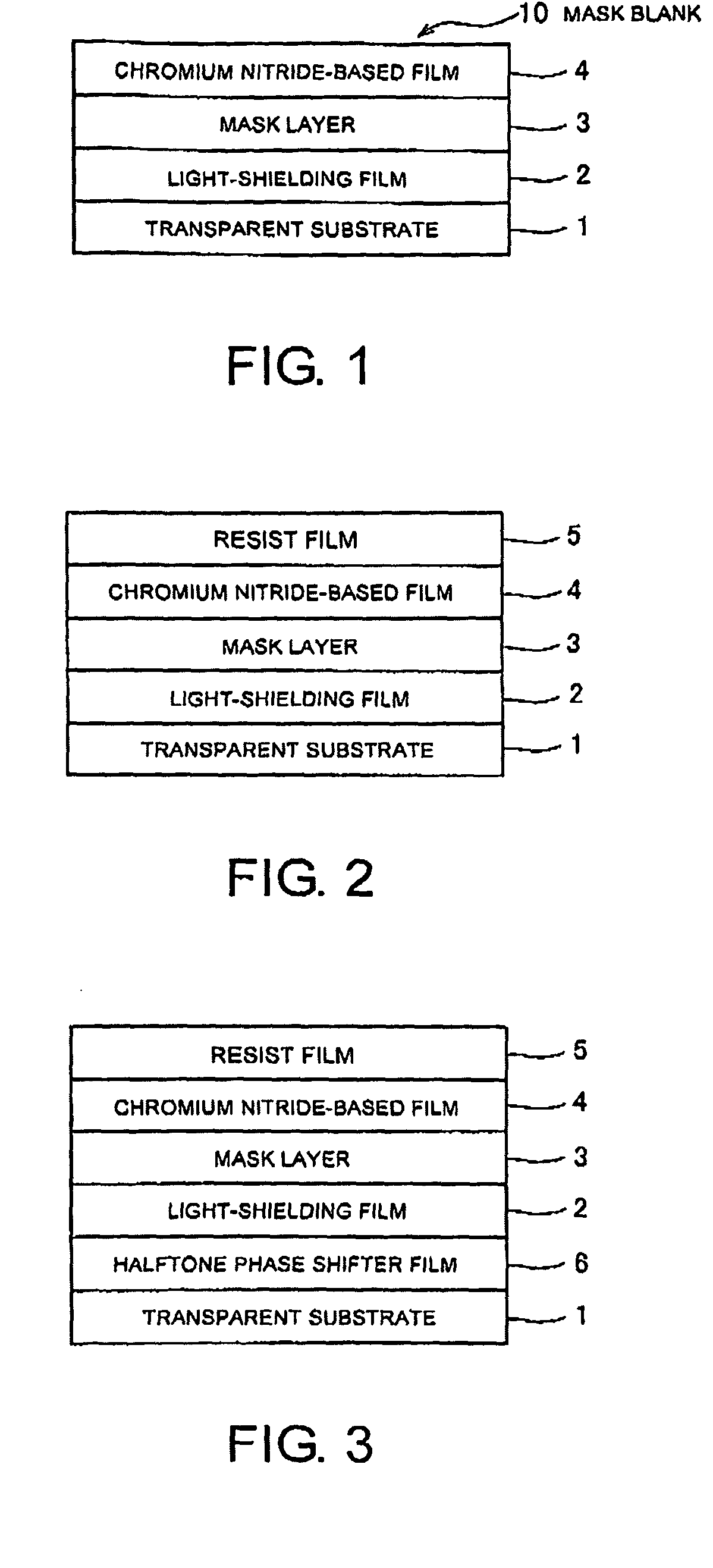
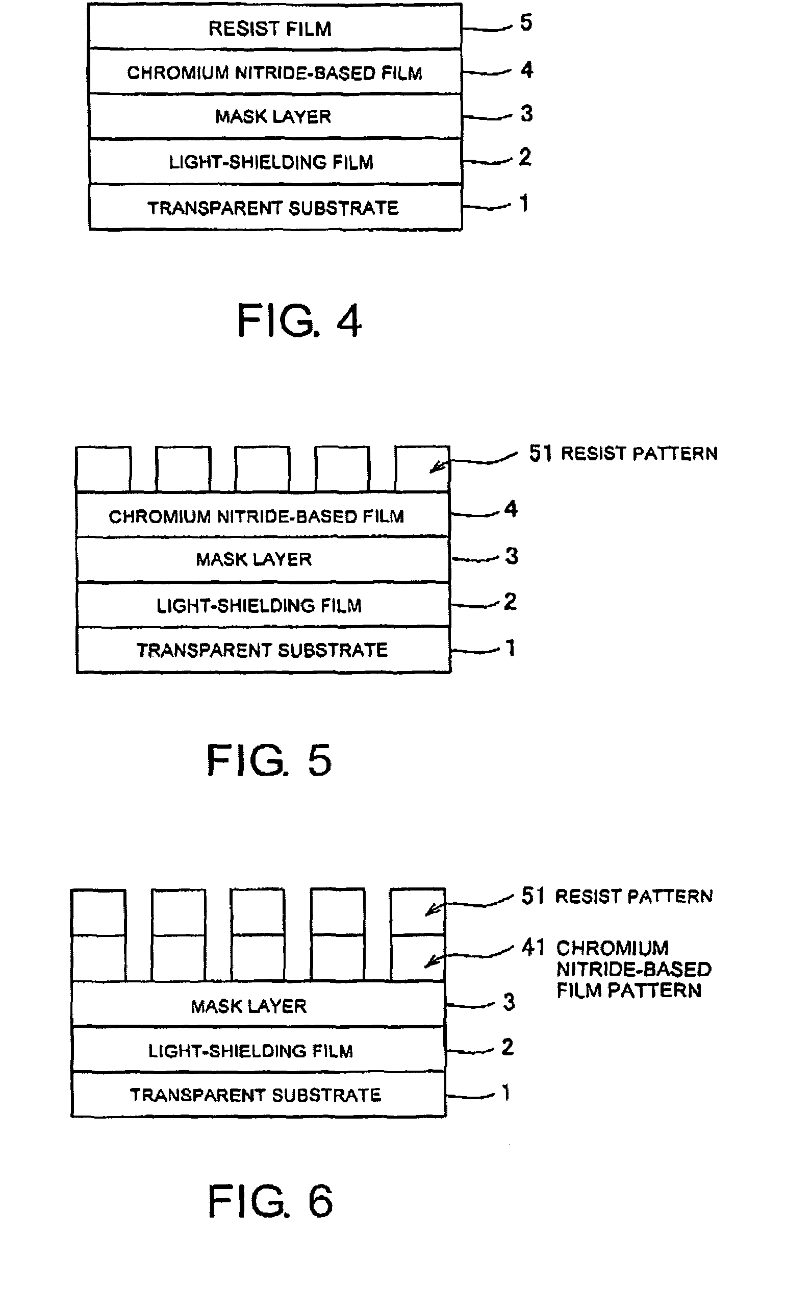
[0036]FIG. 1 is an explanatory diagram of a section of a mask blank according to a first embodiment of this invention. In FIG. 1, symbol 10 denotes the mask blank according to this embodiment. The mask blank 10 comprises a transparent substrate 1 and a light-shielding film 2, a mask layer 3, and a chromium nitride-based film 4 that are formed in this order on the transparent substrate 1. The light-shielding film 2 is a film comprising at least one layer made of a material that can be etched with a dry etching gas containing a chlorine gas. The mask layer 3 formed on the light-shielding film 2 is a film having resistance to etching of the light-shielding film 2. For example, the mask layer 3 is a film that can be etched by a dry etching gas containing a fluorine gas while remains during patterning of the light-shielding film 2 so as to serve as an etching mask. On this mask layer 3, there is formed the chromium nitride-based film 4 made of a material containing at least chromium and ...

second embodiment

[0044]FIG. 2 is an explanatory diagram of a section of a mask blank according to a second embodiment of this invention. The mask blank according to this embodiment has a resist film 5 formed on a chromium nitride-based film 4. The resist film 5 is specifically an electron beam writing resist film. The thickness of the resist film 5 is preferably as thin as possible for achieving high pattern accuracy (CD accuracy) of a light-shielding film 2. Specifically, the thickness of the resist film 5 is preferably 400 nm or less and is more preferably 300 nm or less, 200 nm or less, or 150 nm or less.

[0045]The lower limit of the thickness of the resist film 5 is set so that the resist film 5 remains while dry-etching the lower-layer chromium nitride-based film 4 using as an etching mask a resist pattern formed by applying writing and development processes to the resist film 5. Taking these points into account, the thickness of the resist film 5 is preferably set to 50 nm to 400 nm. For achiev...

third embodiment

[0046]FIG. 3 is an explanatory diagram of a section of a mask blank according to a third embodiment of this invention. The mask blanks according to the foregoing first and second embodiments are each a so-called binary mask blank. However, this invention is also applicable to a mask blank for use in the manufacture of a halftone phase shift mask. The mask blank according to this embodiment shown in FIG. 3 is a mask blank for use in the manufacture of a halftone phase shift mask, wherein a halftone phase shifter film 6 is formed between a transparent substrate 1 and a light-shielding film 2. In this case, it may be configured that a required optical density (e.g. 2.5 or more) is obtained by a combination of the halftone phase shifter film 6 and the light-shielding film 2. In this event, the optical density of the light-shielding film 2 itself can be set to 0.5 or more and, preferably, can be adjusted between 0.5 to 2.5.

[0047]The halftone phase shifter film 6 transmits light with an i...


PUM

PropertyMeasurementUnit
thicknessaaaaaaaaaa
thicknessaaaaaaaaaa
thicknessaaaaaaaaaa

Abstract

A mask blank is formed on a transparent substrate with a light-shielding film of a material mainly containing chromium and is used for obtaining a photomask by forming the light-shielding film into a transfer pattern by lithography using an electron beam writing resist. The mask blank includes a mask layer formed on the light-shielding film for serving as an etching mask in etching that forms the light-shielding film into the transfer pattern. The mask layer is made of a material containing silicon. The mask blank further includes a chromium nitride-based film formed on the mask layer and containing at least chromium and nitrogen.

Description

[0001]This application is based upon and claims the benefit of priority from Japanese patent application No. 2007-239953, filed on Sep. 14, 2007, the disclosure of which is incorporated herein in its entirety by reference.BACKGROUND OF THE INVENTION[0002]This invention relates to a mask (photomask) for use in transferring a fine pattern in the manufacture of semiconductor elements or the like and further relates to a mask blank being a base of such a mask.[0003]With the increase in fineness of circuit patterns of semiconductor elements or the like, the tolerance between designed and measured pattern line widths of photomasks has become much smaller. As the degree of integration of semiconductor integrated circuits has increased, the design rule in the process of manufacturing those circuits has become stricter and more and more stringent demands have been made on the CD (Critical Dimension) uniformity and the CD linearity.[0004]Techniques intended to satisfy such demands are disclos...

Claims


Application Information

Patent Timeline
Patent Type & Authority Patents(United States)
IPC IPC(8): G03F1/00G03F7/00G03F1/32G03F1/54G03F1/68H01L21/027
CPCG03F1/54G03F1/78G03F1/80G03F7/2063G03F1/50
Inventor OKUBO, YASUSHIHASHIMOTO, MASAHIROSUZUKI, TOSHIYUKIOHNISHI, TAKAYUKIANZE, HIROHITOSUNAOSHI, HITOSHIKAMIKUBO, TAKASHI
Owner HOYA CORP
Features
  • R&D
  • Intellectual Property
  • Life Sciences
  • Materials
  • Tech Scout
  • Unparalleled Data Quality
  • Higher Quality Content
  • 60% Fewer Hallucinations
Learn More