Vectorless IVD analysis prior to tapeout to prevent scan test failure due to voltage drop

a scan test and analysis method technology, applied in error detection/correction, program control, instruments, etc., can solve problems such as increasing the likelihood of transistors, increasing the integrity of power supplies, and increasing the possibility of power supply drooping, so as to improve the testability of integrated circuits and avoid long test vector generation processes. , the effect of avoiding the associated delay

Inactive Publication Date: 2013-04-02
APPLE INC
View PDF13 Cites 4 Cited by
  • Summary
  • Abstract
  • Description
  • Claims
  • Application Information

AI Technical Summary

Benefits of technology

[0011]Because the methodology is vectorless, the lengthy test vector generation process and its associated delays may be avoided. While the analysis may be based on a theoretical worst-case test vector that might not actually be generated in the test vector generation process, IVD issues that are detected using the methodology are at least possible in the test vectors and thus could be issues that present problems during the testing of the actual integrated circuit chips. Accordingly, through the early identification and correction of such issues, better testability of the integrated circuit may be realized in some embodiments.

Problems solved by technology

The increase in the number of transistors increases the likelihood that a given instance of the integrated circuit may have a manufacturing flaw that prevents the integrated circuit from operating as designed.
Additionally, the reduced size of the transistors also decreases the minimum size of a flaw that can cause incorrect operation.
An additional issue that requires analysis in the design of integrated circuits is the integrity of the power supply.
As the number of transistors in the integrated circuit increases, the potential for power supply droop to be an issue increases as well.
That is, the impedance characteristics of the power supply distribution interconnect in the integrated circuit, and even the package impedance effects, coupled with localized high current loads due to switching can cause local droop in the magnitude of the supply voltage.
Such droops can slow the operation of the circuitry, and even cause functional failure.
The testing operations can cause switching noise and voltage droop on the power supply, since the circuitry connected to the clocked storage devices reacts to the shifting states.
In some cases, the voltage droop can be severe enough that incorrect operation occurs.
If incorrect operation occurs due to voltage droop, then the circuitry that experiences the voltage droop cannot be tested successfully.
The procedures to generate the test patterns for scan testing are long latency, and thus are typically only performed at or near tapeout of an integrated circuit design, when the scan chains are essentially finalized.
Accordingly, IVD testing often occurs months after the tapeout, when it is no longer possible to make changes to the current integrated circuit design.
Changes must wait for a subsequent tapeout, or in the case that the tapeout is for production, changes are no longer possible for that design.
While the analysis may be based on a theoretical worst-case test vector that might not actually be generated in the test vector generation process, IVD issues that are detected using the methodology are at least possible in the test vectors and thus could be issues that present problems during the testing of the actual integrated circuit chips.

Method used


Image

  • Vectorless IVD analysis prior to tapeout to prevent scan test failure due to voltage drop
  • Vectorless IVD analysis prior to tapeout to prevent scan test failure due to voltage drop
  • Vectorless IVD analysis prior to tapeout to prevent scan test failure due to voltage drop

Examples


Embodiment Construction

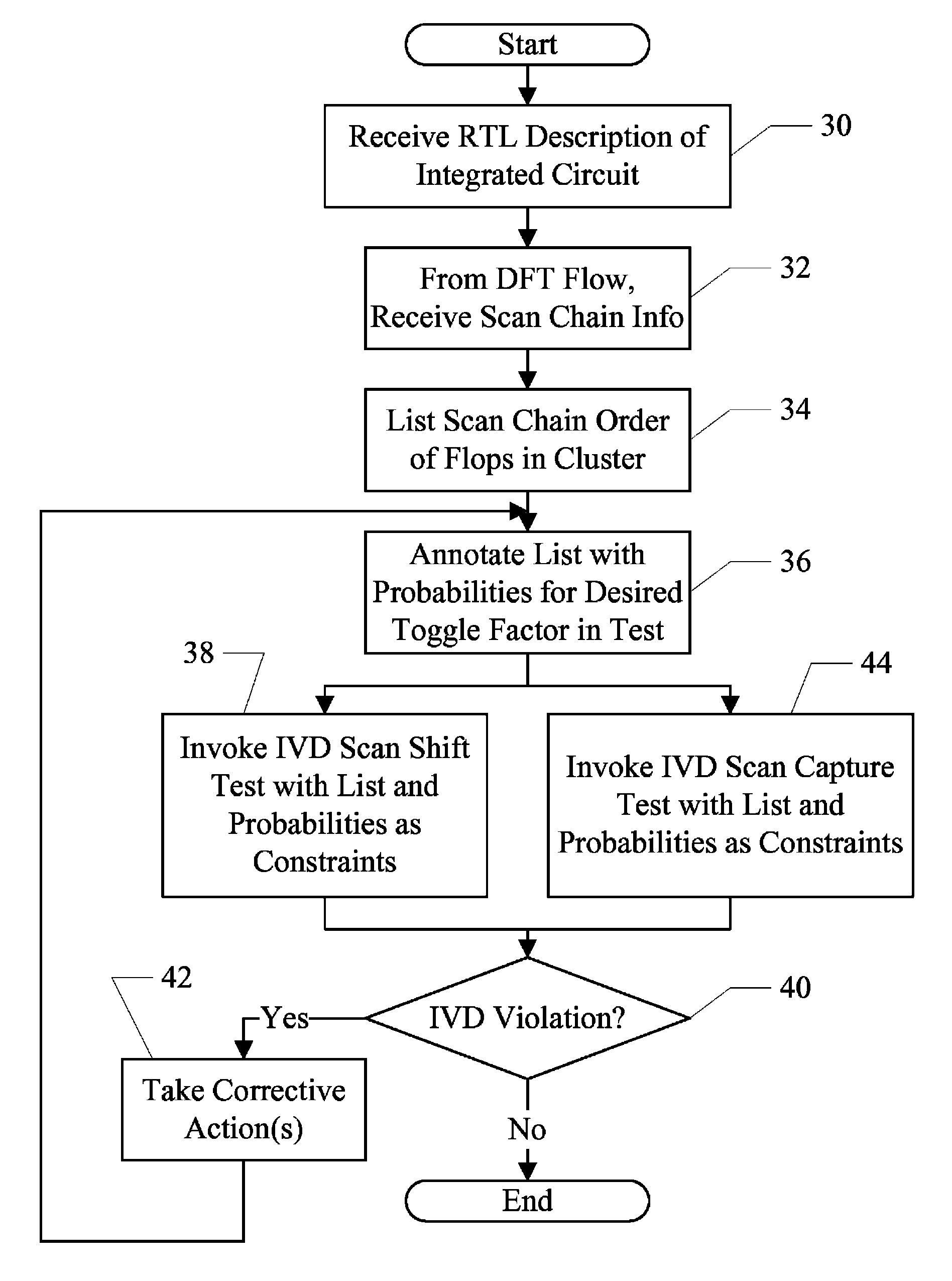
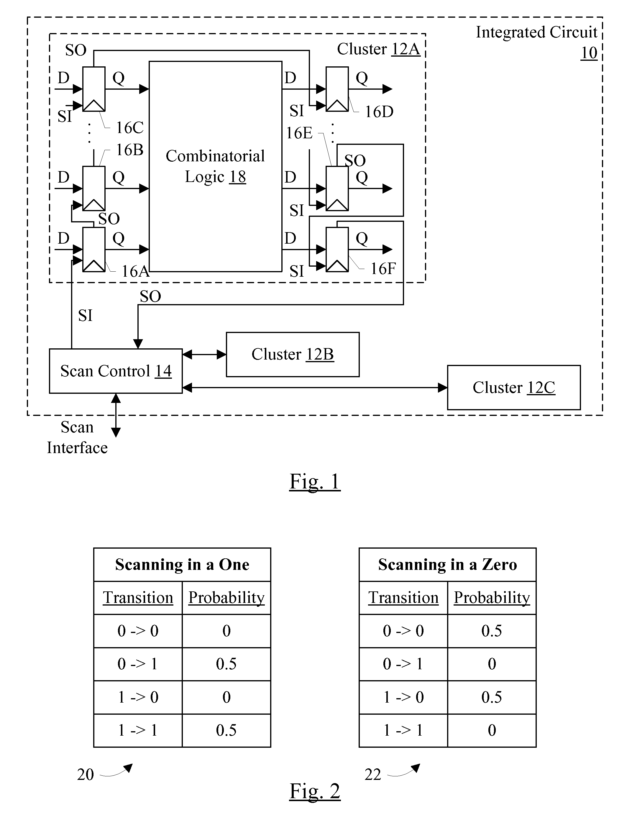
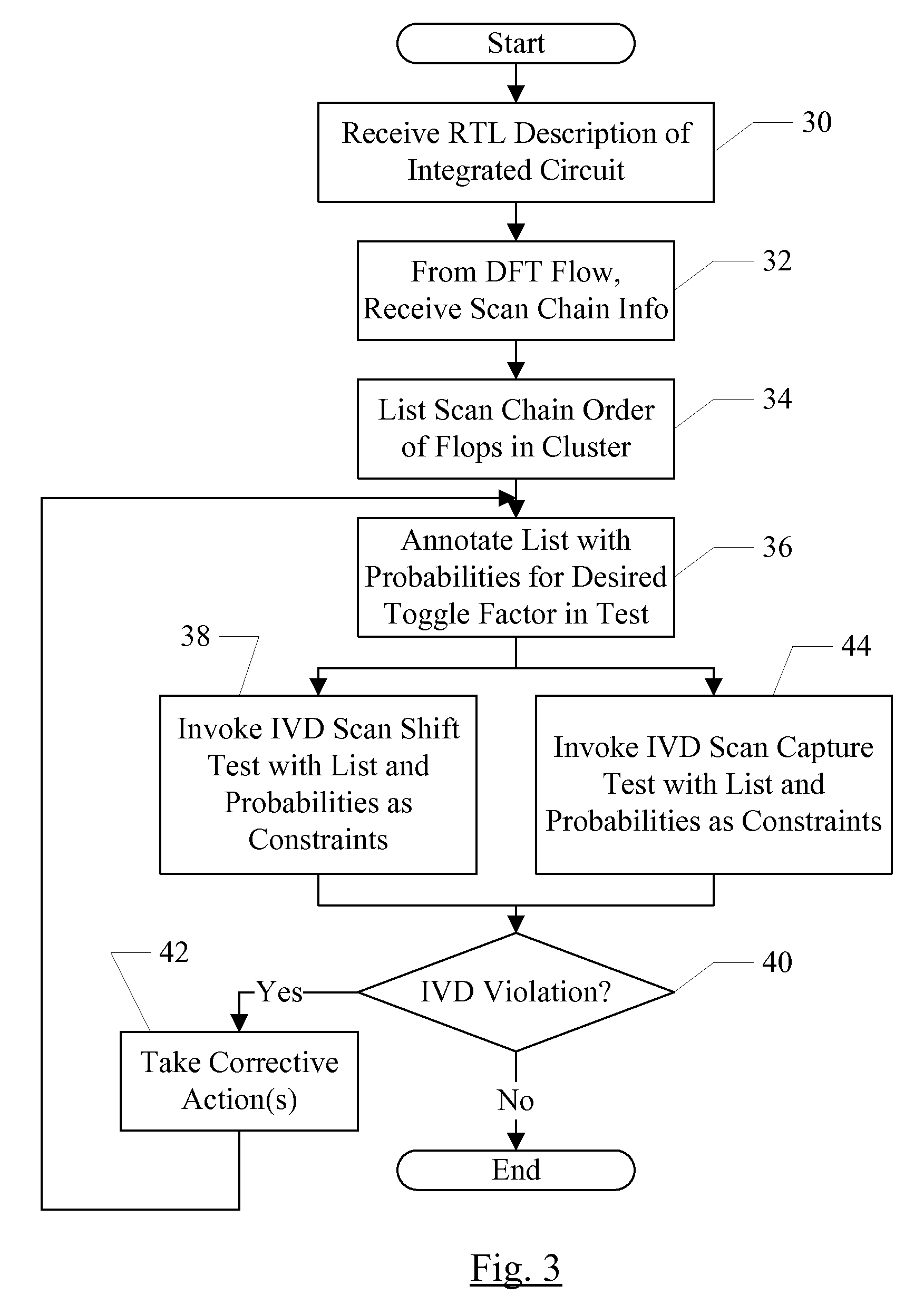
[0021]Turning now to FIG. 1, a block diagram of one embodiment of an integrated circuit 10 is shown. In the illustrated embodiment, the integrated circuit 10 includes multiple circuit clusters 12A-12C coupled to a scan control circuit 14. The scan control circuit 14 is coupled to an external scan interface. The scan interface may be compatible with an industry standard interface such as the test access port (TAP) described in the Institute of Electrical and Electronic Engineers (IEEE) specification 1149.1 and / or 1500, or may be an interface defined by the designers of the integrated circuit 10. Each cluster 12A-12C may include one or more scan chains, beginning with a scan in signal (SI) from the scan control circuit 14 to the cluster 12A-12C and ending with a scan out (SO) signal from the cluster 12A-12C to the scan control circuit 14. For example, one scan chain for the cluster 12A is shown in FIG. 1, although a given cluster may have multiple scan chains.

[0022]Generally, a cluste...


PUM


Abstract

In one embodiment, a vectorless IVD methodology may be used to estimate IVD issues for an integrated circuit earlier in the design cycle of the integrated circuit, e.g. when corrective actions may still be taken to correct IVD failures. In the methodology, scan chains for various clusters in the integrated circuit may be identified, even though the scan chains may still be subject to change as the design evolves. A power integrity tool may analyze the scan chains based on a probability of transitions in the devices within the scan chain (e.g. flops) for a theoretical worst-case test vector. If the result of analysis identifies IVD failures in the clusters, corrective action may be taken such as modifying the design. Alternatively, the corrective action may include identifying one or more flops that experience failure as devices to be excluded from the test vector generation process for scan testing.

Description

BACKGROUND[0001]1. Field of the Invention[0002]This invention is related to integrated circuit design methodology and, more particularly, to ensuring testability of the integrated circuit in manufacture.[0003]2. Description of the Related Art[0004]As semiconductor fabrication technology continues to reduce the size of transistors fabricated on an integrated circuit “chip,” the number of transistors included on a given integrated circuit continues to increase. The increase in the number of transistors increases the likelihood that a given instance of the integrated circuit may have a manufacturing flaw that prevents the integrated circuit from operating as designed. Additionally, the reduced size of the transistors also decreases the minimum size of a flaw that can cause incorrect operation.[0005]To avoiding shipping a flawed integrated circuit to a customer, various schemes to test the integrated circuit during manufacturing (e.g. at the foundry which implements the fabrication proc...

Claims


Application Information

Patent Timeline
Patent Type & Authority Patents(United States)
IPC IPC(8): G06F9/455G06F17/50
CPCG06F17/5081G01R31/318533G06F30/398
Inventor YANG, WEN-CHIEH JEFFREY
Owner APPLE INC
Why Eureka
Try Eureka