Optical I/O array module and its fabrication method

a technology of array modules and optical elements, applied in the direction of optical elements, semiconductor lasers, instruments, etc., can solve the problems of increasing the number of components, increasing the manufacturing cost of a member for obtaining high accuracy, and increasing the difficulty of ensuring a production yield for enabling stable optical linkage to be obtained, so as to achieve high accuracy and stable optical linkage, the effect of fewer components and easy manufacturing

Inactive Publication Date: 2013-05-07
HITACHI LTD
View PDF12 Cites 26 Cited by
  • Summary
  • Abstract
  • Description
  • Claims
  • Application Information

AI Technical Summary

Benefits of technology

[0010]It is therefore an object of the invention to provide an optical I / O array module capable of attaining highly accurate and stable optical linkage between an optical element, and an optical waveguide in a transmission device for batch processing massive amounts of light signals while being easily manufactured with fewer components, increasing a transmission speed per a channel by shortening a distance between the optical element, and an LSI as much as possible, adopting a structure for reducing power consumption, and easily removing an LSI, and a component from the viewpoint of practicality, and a transmission device using the optical I / O array module, and a method for fabricating the same.
[0012]According to an aspect of the present invention, the convex shaped member or the concave shaped member is placed at the spots above the respective mirror parts, and the laser diode array, and the photo diode array, provided with the concave shape, or the convex shape, respectively, are placed on the top of the convex shaped member or the concave shaped member, respectively, thereby causing fitting with each other, so that it is possible to implement highly accurate mounting of the optical elements, using fewer components, with ease. Furthermore, since the optical elements can be mounted with high precision, bonding between the optical elements, and the optical waveguide can be effected at a low loss, so that it is possible to realize efficient and high-quality optical transmission at low power consumption.
[0013]Further, as electrical connection between the optical element, and the driver IC, the amplifier IC, or an LSI incorporating those circuit ICs can be effected by thin-film interconnects covering a short distance, it is possible to increase a transmission speed per channel while preventing an increase in power consumption. Furthermore, LSIs can be mounted by use of the conventional and simple techniques such as solder-bonding or the like, and assembling can be executed with ease while no special technique is required for removal of the LSIs.
[0014]Thus, the present invention can provide an optical I / O array module large in transmission capacity, operable at low power consumption, and capable of reduction in the number of components, and the number of fabricating process steps to thereby attain reduction in cost.

Problems solved by technology

For this reason, mounting tolerance in concurrently meeting positioning accuracy of each optical component is small, so that there are limitations to capability of ensuring excellent optical performance simply by depending on accuracy in fabrication•mounting of members made up of separate components such as pins, sockets, and so forth, and there will result an increase in the number of components, and a rise in the fabrication cost of a member for obtaining high accuracy.
Further, in the case where the optical element and the optical waveguide each are rendered to serve as a multi-channel, it will be increasingly difficult to secure a production yield for enabling stable optical linkage to be obtained.
Even if a transmission speed of a signal from the LSI is increased, the interval acts as a rate-controlling factor, thereby preventing a satisfactory transmission speed from being obtained.
Further, a loss will increase to the extent of an increase in length of the electrical interconnect, thereby raising the risk of an increase in power consumption.
Furthermore, it is not possible to increase packaging density to a sufficiently high level either, thereby inviting an increase in the size of a board.
As to positioning accuracy of the optical element as well as the optical signal transmission line, if an attempt is made for efficient positioning of all channels, this will cause bonding parts to be subjected to a large stress when positional tolerance of respective guide pins as well as respective socket pins are taken into consideration, so that significant deterioration in reliability is anticipated.

Method used


Image

  • Optical I/O array module and its fabrication method
  • Optical I/O array module and its fabrication method
  • Optical I/O array module and its fabrication method

Examples


first embodiment

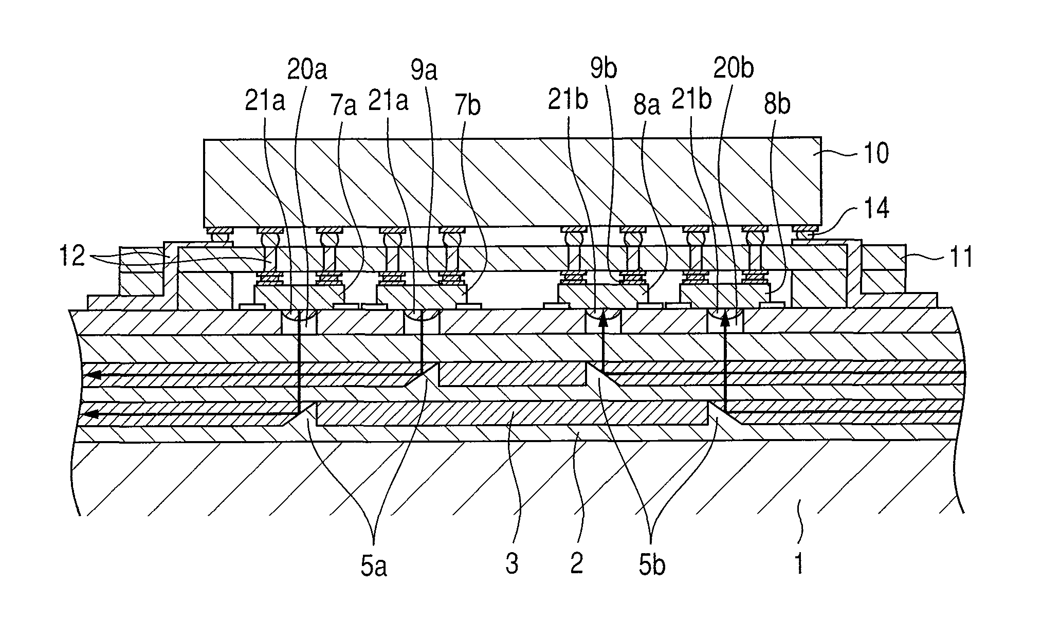
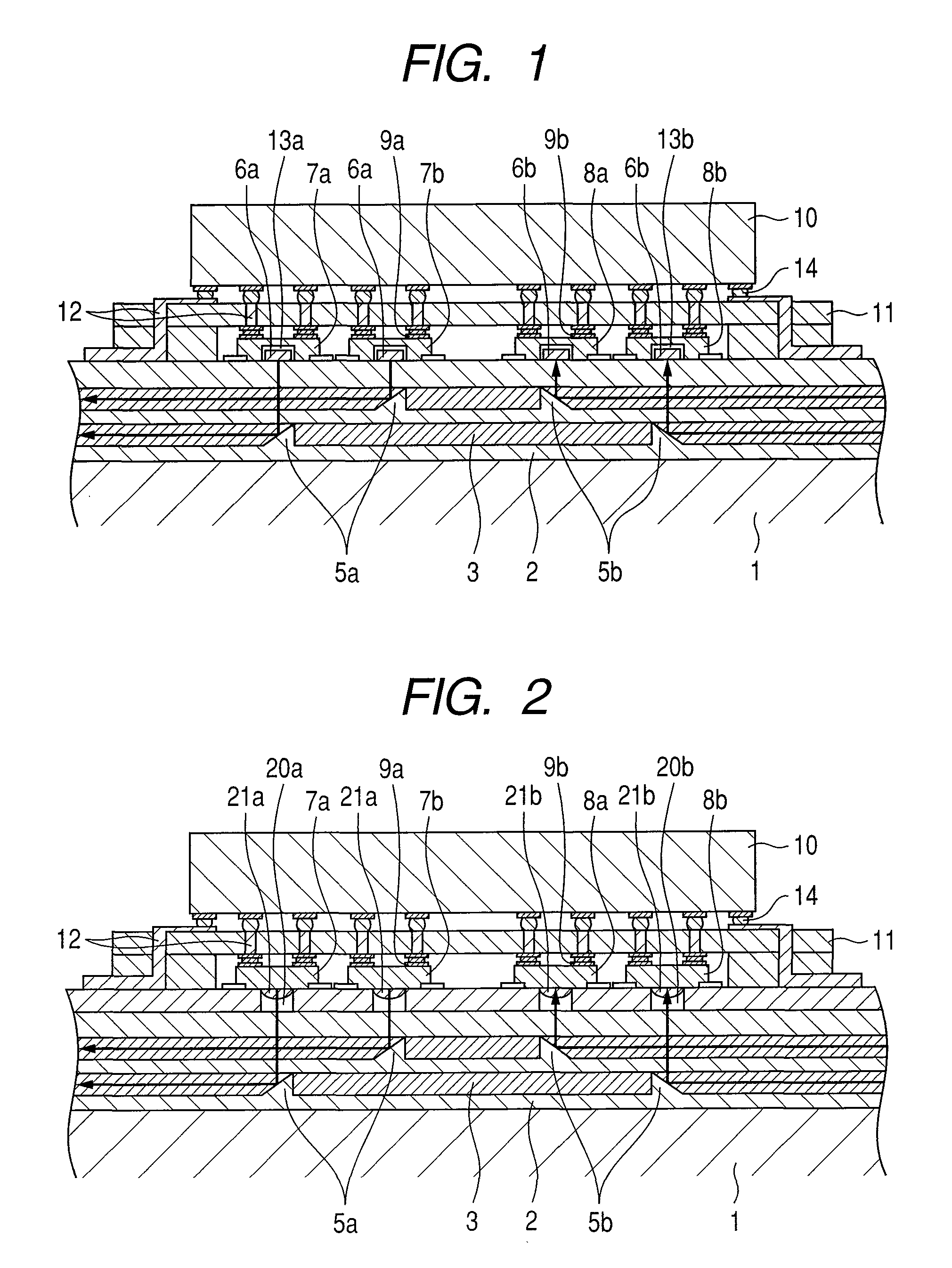
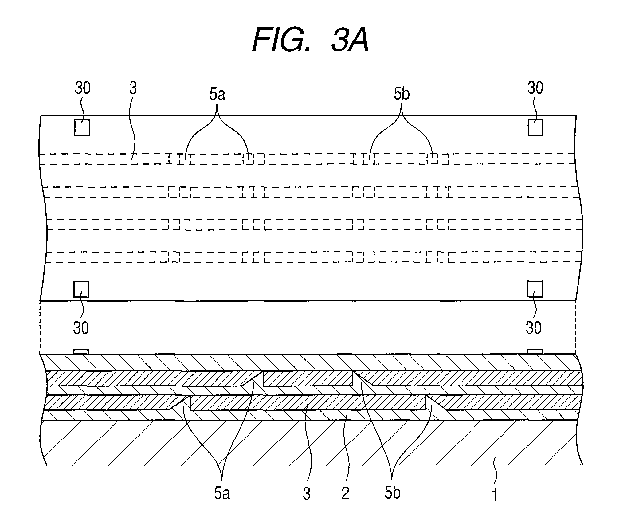
[0032]First, in FIG. 1, there is shown a first embodiment of the present invention. FIG. 1 is a sectional view showing an optical I / O array module according to the present invention. An optical waveguide (core) 3 for use in propagation of a optical signal is provided in such a way as to be covered by a clad 2 on a substrate 1 made up of FR-4, and so forth, and mirror parts 5a, 5b, each having a face tapered at an angle of 45°, are formed at optional spots of the optical waveguide 3, respectively. With the present embodiment, the optical waveguide 3 is formed in two layers in order to enhance packaging density, but it may be formed in a single layer, or three or more layers instead. Further, convex shaped members 6a, 6b are provided on the top surface of the substrate 1, and directly above the mirror parts 5a, 5b, respectively

[0033]In this connection, there is no limitation to the convex members 6a, 6b as long as the convex members 6a, 6b each have transparency against the wavelength...

second embodiment

[0047]Now, a procedure of fabricating a laser diode array to be mounted in an optical I / O array module according to a second embodiment of the invention is described by way of example with reference to FIGS. 4A to 4D, respectively.

[0048]FIG. 4A is view showing a state in which a epitaxial layer 41 is formed on the top of a semiconductor substrate 40. As a constituent material of the semiconductor substrate 40, there are cited gallium arsenide (GaAs), indium phosphide (InP), and so forth, commonly used in an optical element of a compound semiconductor, and use is preferably made of a material having transparency against an emission light wavelength lest a loss occurs upon light passing through the semiconductor substrate 40.

[0049]Next, as shown in FIG. 4B, a forming process such as the photolithography, etching, and so forth is applied to the epitaxial layer 41 to thereby form light emission parts 42. A mirror structure, and so forth are provided inside, or in the vicinity of the lig...

third embodiment

[0052]Next, there is described a third embodiment of the invention with reference to FIG. 5. FIG. 5 is a sectional view showing an optical I / O array module according to the third embodiment of the invention. With the present structure of the optical I / O array module, a protrusion 50 made up a portion of a filmy layer 11 is provided at the midpoint spot between laser diode arrays 7a, 7b, and photo diode arrays 8a, 8b. With the adoption of the present structure, the laser diode arrays 7a, 7b, and the photo diode arrays 8a, 8b come to be hemmed in respective enclosed spaces inside the filmy layer 11 to be thereby sealed from outside of the module, so that it is possible to lessen deterioration in optical elements, taking place over time due to adhesion of moisture, and foreign particles. The enclosed space may be hermetically sealed from outside air, however, even if the enclosed space is filled up with a transparent resin or the like, thereby making up a non-hermetically sealed struct...


PUM

PropertyMeasurementUnit
angleaaaaaaaaaa
visible transparencyaaaaaaaaaa
opticalaaaaaaaaaa

Abstract

In fabricating an optical I / O array module, an optical waveguide provided with mirror parts, each having a tapered face, is formed on a substrate, a convex shaped member or a concave shaped member is placed at spots above the respective mirror parts of the optical waveguide, and laser diode arrays and photo diode arrays, provided with either a concave shape, or a convex shape, are mated with, or into the convex shaped member or the concave shaped member before being mounted. Further, there are formed multiple filmy layers, on which an LSI where a driver IC LSI of optical elements, and an amplifier LSI of the optical elements are integrated.

Description

CLAIM OF PRIORITY[0001]The present application claims priority from Japanese patent application JP 2009-175635 filed on Jul. 28, 2009, the content of which is hereby incorporated by reference into this application.FIELD OF THE INVENTION[0002]The present invention relates to an optical I / O array module for batch processing massive amounts of optical signals that are transmitted and received in an intra-rack, the transmission equipment using the same, and a method for fabricating the same.BACKGROUND OF THE INVENTION[0003]Recent years have seen rapid advances in servicing of communication traffic by optical signals in the field of information and telecommunications, and there has so far been developed a fiber-optic network, such as the backbone, metropolitan, and access systems, over a relatively long distance at least several km. In order to process massive amounts of data travelling over a shorter distance such as rack-to-rack (in a range of several to several hundreds of m), or a di...

Claims


Application Information

Patent Timeline
Patent Type & Authority Patents(United States)
IPC IPC(8): G02B6/26G02B6/42
CPCG02B6/43G02B6/4214G02B6/423Y10T29/49117H01S5/423
Inventor MATSUOKA, YASUNOBUSUGAWARA, TOSHIKIADACHI, KOICHIROMATSUSHIMA, NAOKIHAMAMURA, SAORIMINAGAWA, MADOKACHUJO, NORIO
Owner HITACHI LTD
Why Eureka
Try Eureka