Thin film transistor and method of manufacturing the same

a thin film transistor and film technology, applied in the field of thin film transistors, can solve the problems of low heat resistance, difficult to employ flexible substrates, plastic substrates or film substrates, etc., and achieve the effects of preventing current rate control, reducing hot carrier-induced degradation of tft, and small threshold voltage chang

Active Publication Date: 2013-05-21
CANON KK
View PDF23 Cites 95 Cited by
  • Summary
  • Abstract
  • Description
  • Claims
  • Application Information

AI Technical Summary

Benefits of technology

[0019]According to the present invention, source / drain regions are formed by hydrogen diffusion when the interlayer insulating layer is formed with a channel protection layer as a mask, with the result that a coplanar structure TFT in which parasitic resistance between the source / drain regions and the channel region can be reduced can be manufactured. Therefore, according to the present invention, current rate control can be prevented in the coplanar structure TFT.
[0020]Further, the TFT according to the present invention includes regions having resistivity lower than that of a channel region and higher than those of the source / drain regions (hereinafter, referred to as medium-resistance regions) between the channel region and the source / drain regions. Electric field concentration at the source / drain ends is thus relieved and the hot carrier-induced degradation of the TFT can be lessened. This makes the TFT according to the present invention small in threshold voltage change under electrical stress and accordingly high in stability.

Problems solved by technology

The manufacture of those TFTs requires a high temperature process, and hence it is difficult to employ a flexible substrate such as a plastic substrate or film substrate which is low in heat resistance.
This gives rise to such problems as a difficulty in making pixels finer and reducing of the amount of current flowing into an organic EL device by a change in threshold voltage of the TFT after long-hour driving.
Low-temperature poly-silicon TFTs also have the following problems.
Low-temperature poly-silicon TFTs need a correction circuit for solving unevenness that is caused by an excimer laser used to crystallize silicon, resulting in complicating the circuit design.
In addition, increasing the screen size is difficult because the screen size is limited by how large an area an excimer laser can irradiate.
In the case where the plasma-enhanced chemical vapor deposition (CVD) method or the sputtering method is used to form the gate insulating layer, damage caused by plasma to the oxide semiconductor channel layer becomes a problem.
Further, in the case where the gate insulating layer is a silicon nitride film or a silicon oxide film that is formed by the plasma-enhanced CVD method, hydrogen contained in the film diffuses into the oxide semiconductor channel layer, thereby lowering the resistance of the oxide semiconductor.
However, a gate insulating layer that is low in insulating ability raises the gate leakage current of the TFT, and a defect at the interface between the gate insulating layer and the oxide semiconductor layer causes lowering of ON current and an increase in S value.

Method used


Image

  • Thin film transistor and method of manufacturing the same
  • Thin film transistor and method of manufacturing the same
  • Thin film transistor and method of manufacturing the same

Examples


example 1

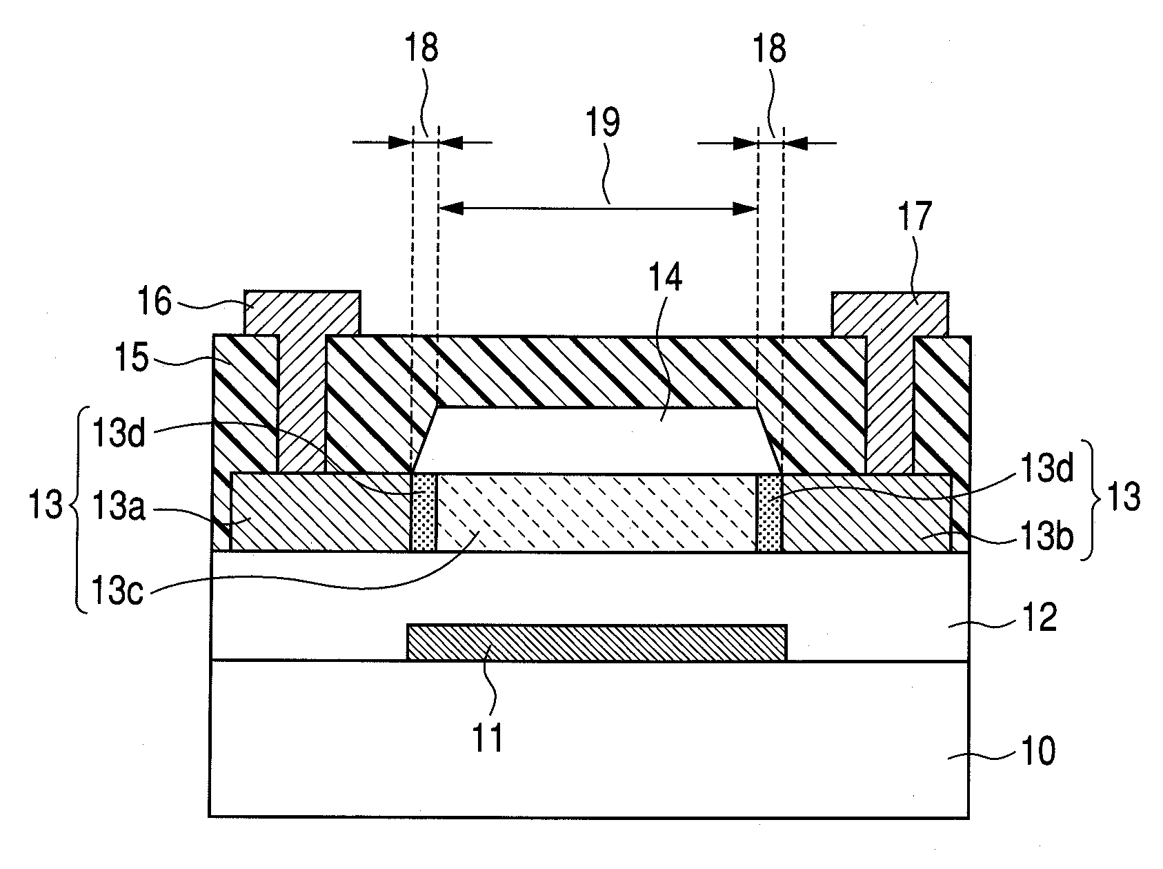
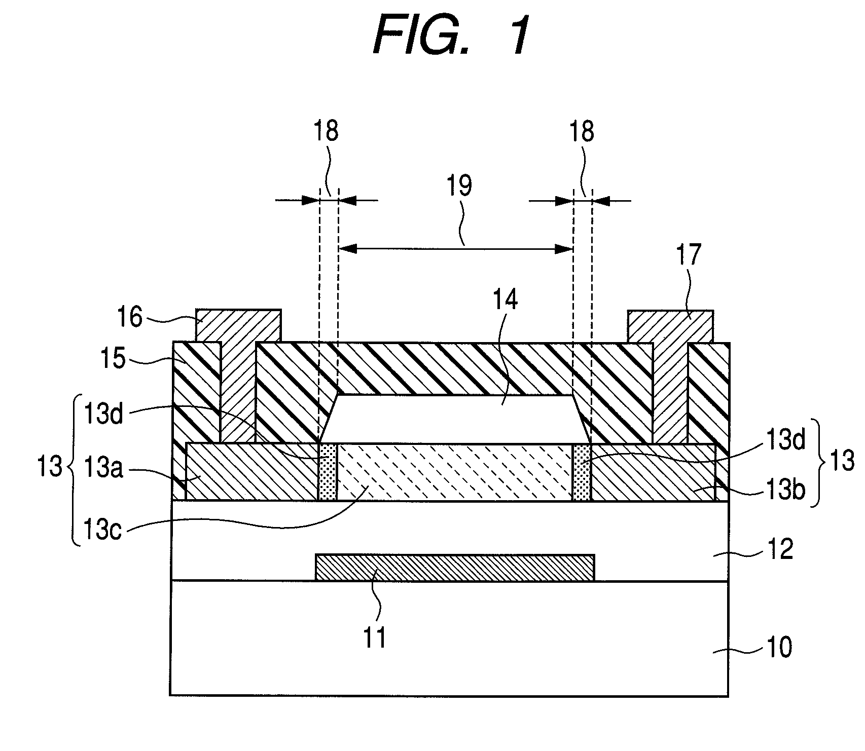
[0081]The bottom gate type coplanar structure oxide semiconductor TFT illustrated in FIG. 1 in which the channel protection layer is a single layer was manufactured in this example.

[0082]First, an electrode layer for forming the gate electrode 11 was formed by the electron beam deposition method on the glass substrate 10 (Corning 1737 manufactured by Corning Incorporated). The electrode material used is Ti / Au / Ti, and the thicknesses of the Ti layer, the Au layer, and the other Ti layer are 5 nm, 40 nm, and 5 nm, respectively.

[0083]After that, the electrode layer was patterned by the photolithography method, thereby obtaining the gate electrode 11.

[0084]A silicon oxide film with a thickness of 200 nm was formed as the gate insulating layer 12 by the sputtering method. In order to form the silicon oxide film, an RF sputtering apparatus was used and the substrate temperature was set to room temperature. A 3-inch diameter SiO2 target was used with the input RF power set to 400 W. During...

example 2

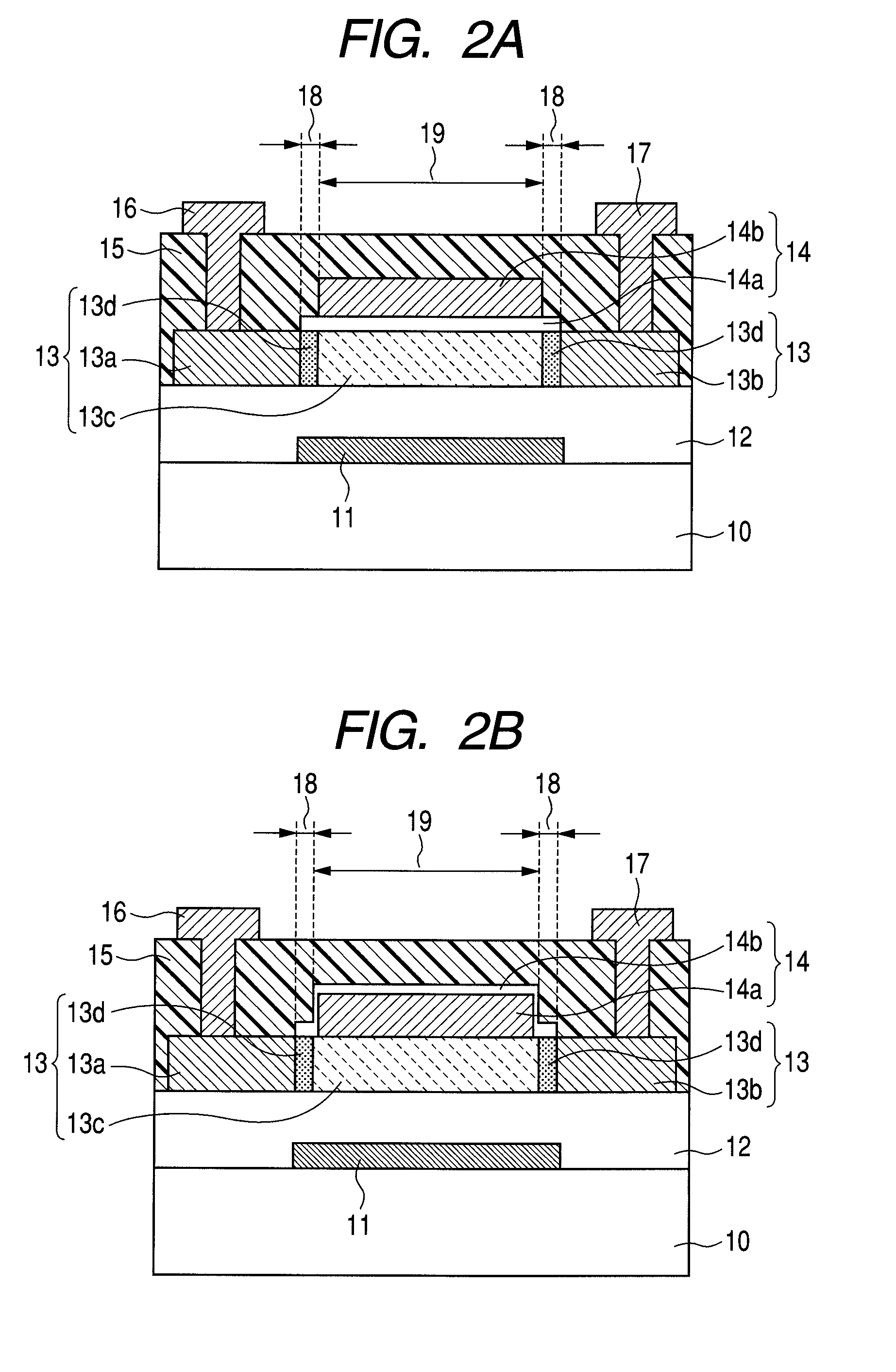
[0094]The bottom gate type coplanar structure oxide semiconductor TFT illustrated in FIG. 2A in which the channel protection layer is formed of two layers was manufactured in this example.

[0095]First, the gate electrode 11, the gate insulating layer 12, and the oxide semiconductor layer 13 are formed on the glass substrate 10 in the same manner as in Example 1.

[0096]On the oxide semiconductor layer 13, a silicon oxide film is formed to have a thickness of 10 nm by the sputtering method as the first channel protection layer 14a. Film formation conditions of the first channel protection layer 14a are the same as those of the channel protection layer 14 of Example 1. The first channel protection layer 14a is then patterned by the photolithography method and the dry etching method.

[0097]A silicon oxide film with a thickness of 300 nm is formed next by the sputtering method as the second channel protection layer 14b. Film formation conditions of the second channel protection layer 14b ar...

example 3

[0102]A display device that uses the bottom gate type coplanar structure oxide semiconductor TFT illustrated in FIG. 8 was manufactured in this example.

[0103]The oxide semiconductor TFT manufacturing steps employed here are the same as those of the above-mentioned Example 1. However, the display device may use any of the oxide semiconductor TFTs illustrated in FIGS. 1, 2A, and 2B. First, a silicon nitride film is formed by the plasma-enhanced CVD method as the insulating layer 128 on the oxide semiconductor TFT 120 of the present invention. A contact hole is formed in the insulating layer 128 by the photolithography method. The electrode 130 is connected to the source wiring line 127 through the insulating layer 128. The electrode 130 is an ITO film formed by the sputtering method. On the electrode 130, the hole transport layer 131a and the light-emitting layer 131b are formed by deposition. α-NPD and Alq3 are used for the hole transport layer 131a and the light-emitting layer 131b,...


PUM


Abstract

Provided are a coplanar structure thin film transistor that allows a threshold voltage to change only a little under electric stress, and a method of manufacturing the same. The thin film transistor includes on a substrate at least: a gate electrode; a gate insulating layer; an oxide semiconductor layer including a source electrode, a drain electrode, and a channel region; a channel protection layer; and an interlayer insulating layer. The channel protection layer includes one or more layers, the layer in contact with the oxide semiconductor layer among the one or more layers being made of an insulating material containing oxygen, ends of the channel protection layer are thinner than a central part of the channel protection layer, the interlayer insulating layer contains hydrogen, and regions of the oxide semiconductor layer that are in direct contact with the interlayer insulating layer form the source electrode and the drain electrode.

Description

TECHNICAL FIELD[0001]The present invention relates to a thin film transistor and a method of manufacturing the same. More particularly, the present invention relates to a thin film transistor that uses an oxide semiconductor and a method of manufacturing the thin film transistor.BACKGROUND ART[0002]Thin film transistors (TFTs) are widely used today as a switching device or a driving device in display devices such as active matrix-type liquid crystal display devices and organic electro-luminescence (EL) display devices. Thin film transistors use, for example, amorphous silicon or low-temperature poly-silicon for a semiconductor layer.[0003]The manufacture of those TFTs requires a high temperature process, and hence it is difficult to employ a flexible substrate such as a plastic substrate or film substrate which is low in heat resistance.[0004]Amorphous silicon TFTs, when used as a driving device, have to be large in size because the field effect mobility in this case is small (to 1 ...

Claims


Application Information

Patent Timeline
Patent Type & Authority Patents(United States)
IPC IPC(8): H01L29/10H01L29/12
CPCH01L29/78621H01L29/7869
Inventor SATO, AYUMUHAYASHI, RYOYABUTA, HISATOSANO, MASAFUMI
Owner CANON KK
Why Eureka
Try Eureka