Mask ROM fabrication method
a mask rom and fabrication method technology, applied in the field of mask rom technology, can solve the problem of hard to reduce the overall area and achieve the effect of hard to further reduce the size of the mask rom
- Summary
- Abstract
- Description
- Claims
- Application Information
AI Technical Summary
Benefits of technology
Problems solved by technology
Method used
Image
Examples
Embodiment Construction
[0033]The embodiments are used to describe the technical contents of the present invention in detail in cooperation with the drawings below.
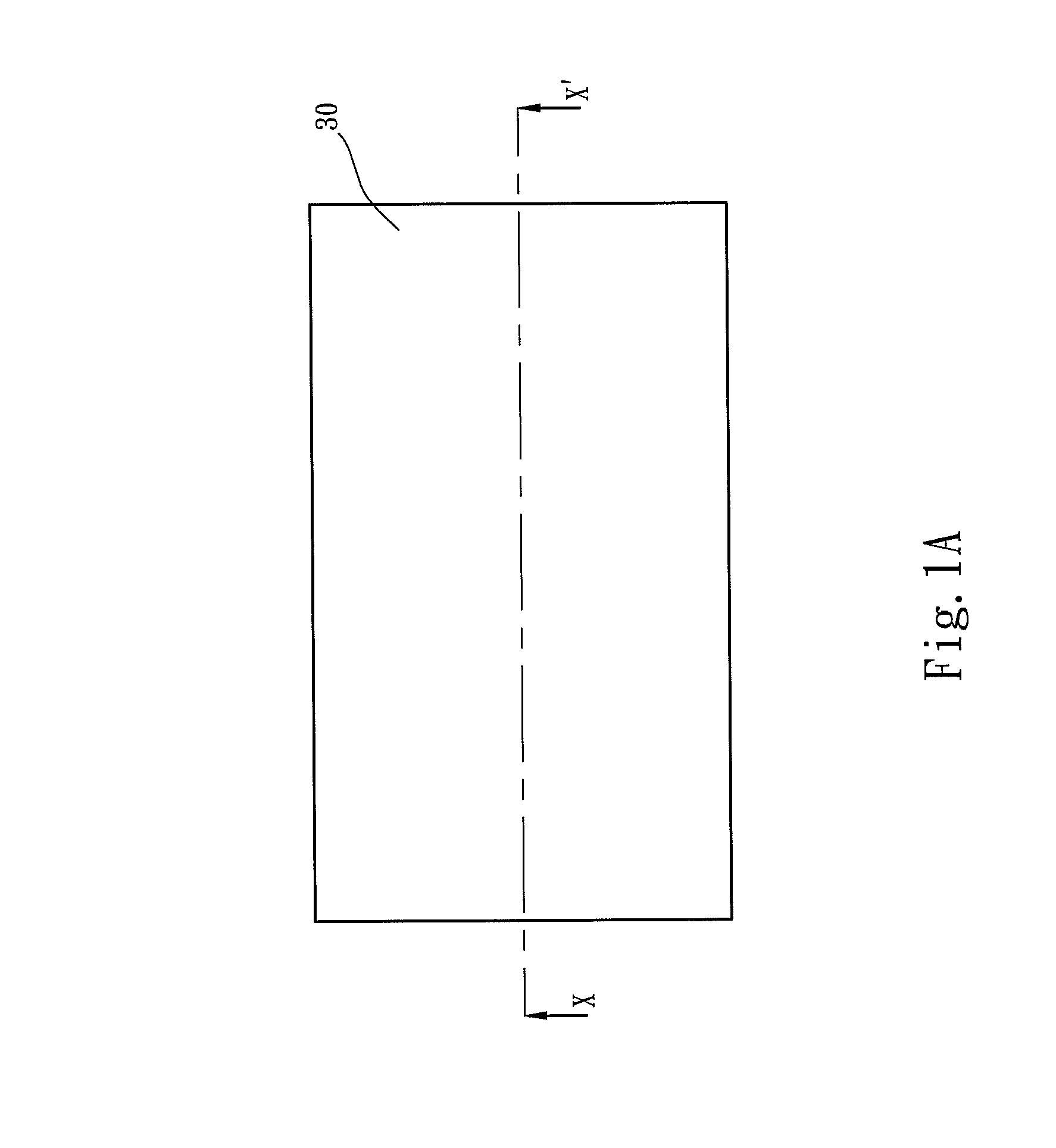
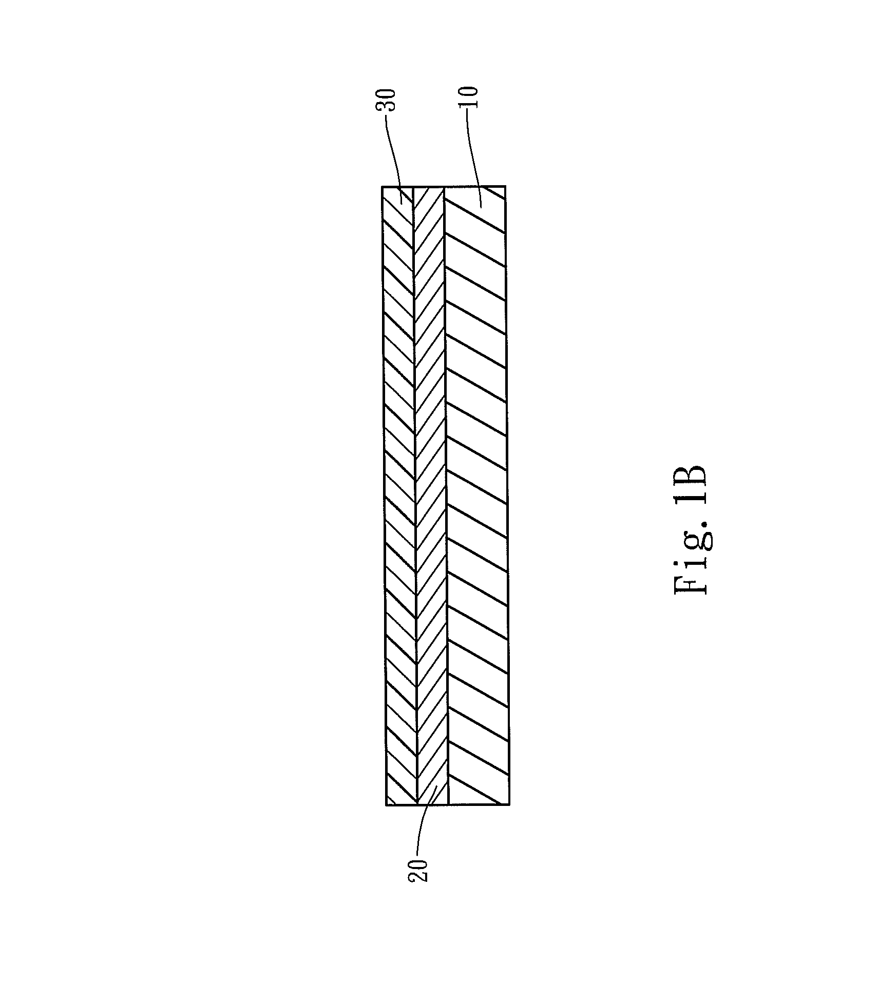
[0034]Refer to FIG. 1A and FIG. 1B. The mask ROM fabrication method of the present invention comprises the following steps.
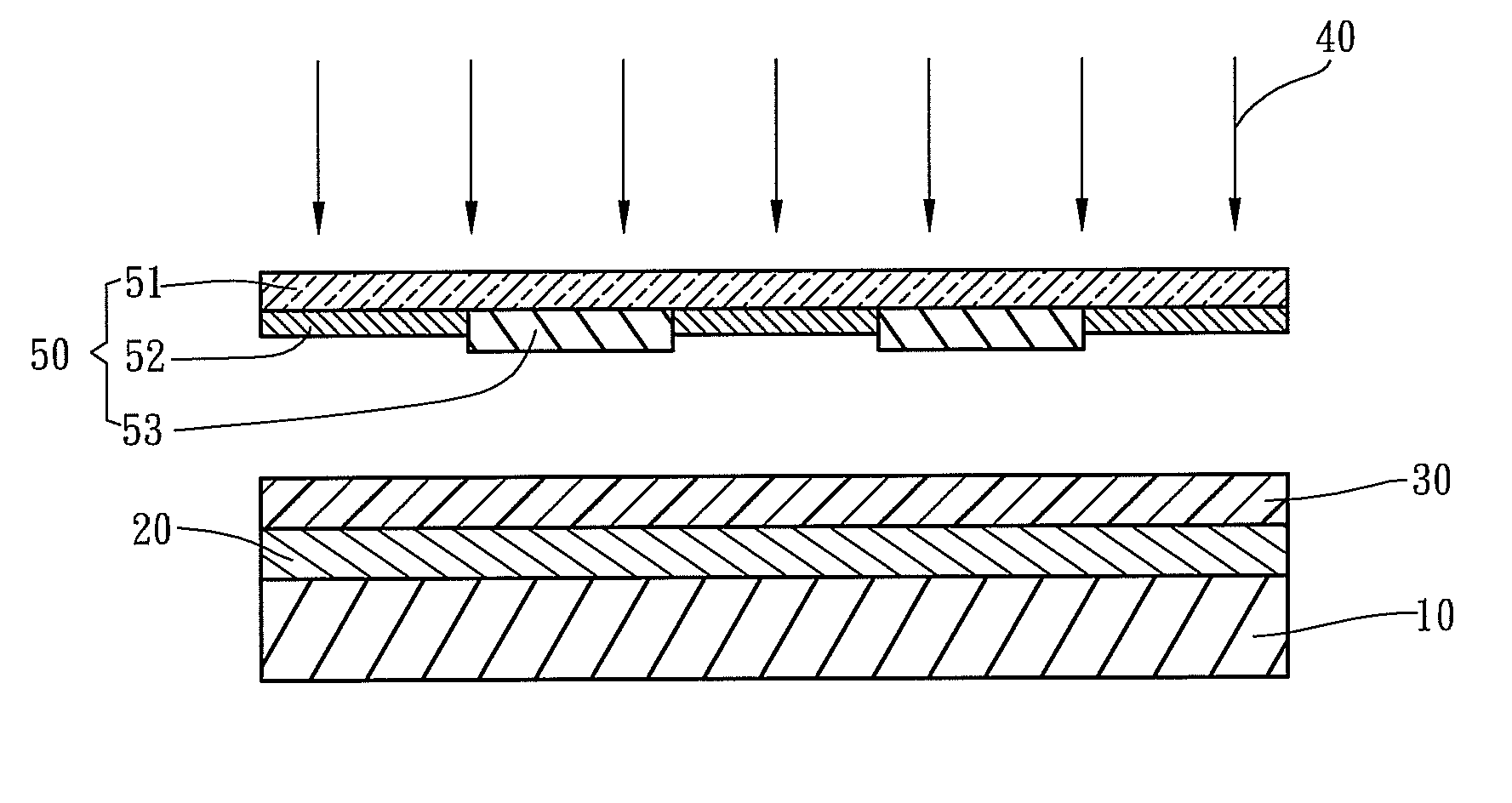
[0035]In Step 1, form a gate dielectric layer 20 on a substrate 10 and a first photoresist layer 30 on the gate dielectric layer 20. In one embodiment, the substrate 10 is a silicon substrate doped with a p-type dopant, wherein the p-type dopant is selected from a group consisting of boron, indium, aluminum, and gallium. Silicon dioxide is grown on the substrate 10 to form the gate dielectric layer 20. Next, photoresist is spin-coated on the gate dielectric layer 20 to form the first photoresist layer 30. In this embodiment, the first photoresist layer 30 is exemplified by a positive photoresist layer. However, a negative photoresist may also be used as the material of the first photoresist layer 30 in the present invention....
PUM
 Abstract
Description
Claims
Application Information


