Semiconductor device manufacturing method thereof

a technology of semiconductor devices and manufacturing methods, applied in semiconductor devices, semiconductor/solid-state device details, electrical apparatus, etc., can solve the problems of increased manufacturing cost, low dopant activation ratio, and inability to process at high temperature, and achieves the effect of reducing manufacturing costs, reducing manufacturing costs, and mechanical strength of wafers

Inactive Publication Date: 2013-08-13
FUJI ELECTRIC CO LTD
View PDF20 Cites 5 Cited by
  • Summary
  • Abstract
  • Description
  • Claims
  • Application Information

AI Technical Summary

Benefits of technology

[0027]In order to solve the above mentioned problems of the prior art, it is an object of the present invention to provide such a semiconductor device as a reverse blocking IGBT, which can form the p-isolation layer at low cost without requiring a glass support substrate and adhesive, and a manufacturing method thereof. It is another object of the present invention to provide a method for manufacturing such a semiconductor device as a reverse blocking IGBT, which can sufficiently activate dopants implanted in the side walls of tapered grooves, of which tilt angle is 60° or more, on the wafer using a simple method without allowing the laser beam to damage the plane where opening portions of the grooves are formed.
[0048]A method for manufacturing a semiconductor device according to Claim 20 of the invention is the invention according to Claim 19, further including a step of removing processing strain, formed in the grooves due to the dicing blade, by etching in a state of the aluminum film remaining, after the grooves are formed with the dicing blade and before implanting the impurity ions.
[0051]According to this invention, in such a semiconductor device as a reverse blocking IGBT, a p-diffusion layer is formed on a front face of the wafer near the dicing region of the wafer, and grooves are formed from the rear face of the wafer to the front face of the wafer, such that the grooves reach the p-diffusion layer but do not reach the front face of the wafer, with a part of the wafer thickness in the bottom portions of the grooves remaining as residual film, whereby the conventionally required glass support substrate is not required, and expensive adhesive for bonding the wafer to the glass support substrate is also not required. Since the glass support substrate and the adhesive are unnecessary, the grooves and p-isolation layer can be formed at low cost.
[0052]By making the depth of the grooves in the outer periphery portion of the wafer to be shallower, or by not forming grooves near the edge portion of the wafer, the mechanical strength of the wafer in the outer periphery portion can be strengthened so that the self-weight of the wafer can be supported by the wafer itself. This makes handling of the wafer easier. By setting the thickness of the residual film to 10 μm or more and strengthening the outer periphery portion of the wafer, the glass support substrate can be unnecessary. By setting the depth of the p-diffusion layer to 170 μm or less, the processing time for the thermal diffusion processing step, which is performed at a high temperature for a long time, can be dramatically reduced, and manufacturing cost and lead time can be decreased.
[0053]If a groove of which opening portion is wider than the bottom portion is formed, the opening portion of the groove is formed when laser annealing is performed using a laser beam under relatively high energy conditions, which are appropriate for activating the dopants implanted in the side wall of the groove, and an aluminum film is formed on the plane (rear face of the ware) where the laser beam is vertically irradiated. Therefore irradiation of the laser beam under relatively high energy conditions onto the rear face of the wafer can be prevented. Since the laser beam having excessive energy is not irradiated onto the rear face of the wafer like this, the generation of abrasion and crystal defects can be prevented, and crystals changing into an amorphous state can be prevented.

Problems solved by technology

Another available method for activating dopants implanted by ion implantation is a furnace annealing processing, but in this case, the processing temperature is limited by the heat resistance temperature of the metal electrode film and protective film already formed on the front face of the wafer, therefore processing at high temperature is not possible, and the dopant activation ratio is low.
In order to form this thick thermal oxide film, thermal oxidation processing must be performed at high temperature for a long time, which increases the manufacturing cost.
The diffusion of dopants requires a lengthy processing time at high temperature, so throughput dramatically drops, and the dopants are inevitably diffused in the lateral direction since the dopants isotropically diffuse from the mask opening portion to the silicon bulk, which causes problems in reducing device pitch and chip size.
The heat treatment time and device pitch are dramatically decreased by this method, but piercing all the way to the front face of the wafer causes separation and individual chips to fall, so the wafer must be bonded with the glass substrate or the like, which makes processing complicated and increases manufacturing cost.
After forming the pierced V grooves (penetrated grooves), ion implantation and laser annealing are performed, but as FIG. 29 shows, adhesive, which bonds the wafer and the glass substrate, is irradiated by the laser beam in portion A, that is a portion where the penetrated grooves (based portion of the V grooves), so a special expensive adhesive, which is not affected by irradiation of the laser beam, must be used, and therefore manufacturing cost increases.
Then the collector electrode is formed by sputtering after laser annealing, but a heat resistant expensive adhesive must be used so as not to be affected even if the adhesive is heated by this sputtering processing, which increases manufacturing cost.
Or an expensive sputtering device having a special cooling mechanism must be used so that the heat temperature does not rise.
Another problem is that the sintering processing temperature, after sputtering, is limited by the heat resistance temperature of the adhesive.
In other words, the manufacturing cost increases if the conventional method is used.
Another problem of RIE etching is that the tilt angle of the side wall of the groove can be decreased only down to about 75°.
This means that with the irradiation energy density conforming to the conditions appropriate for the plane, dopants implanted into the side wall of the tapered groove cannot be activated.
With this however, a laser beam with excessive irradiation energy density is irradiated onto the plane, so abrasion and crystal defects may be generated on the plane, or [crystals] may change into an amorphous state.

Method used


Image

  • Semiconductor device manufacturing method thereof
  • Semiconductor device manufacturing method thereof
  • Semiconductor device manufacturing method thereof

Examples


example 1

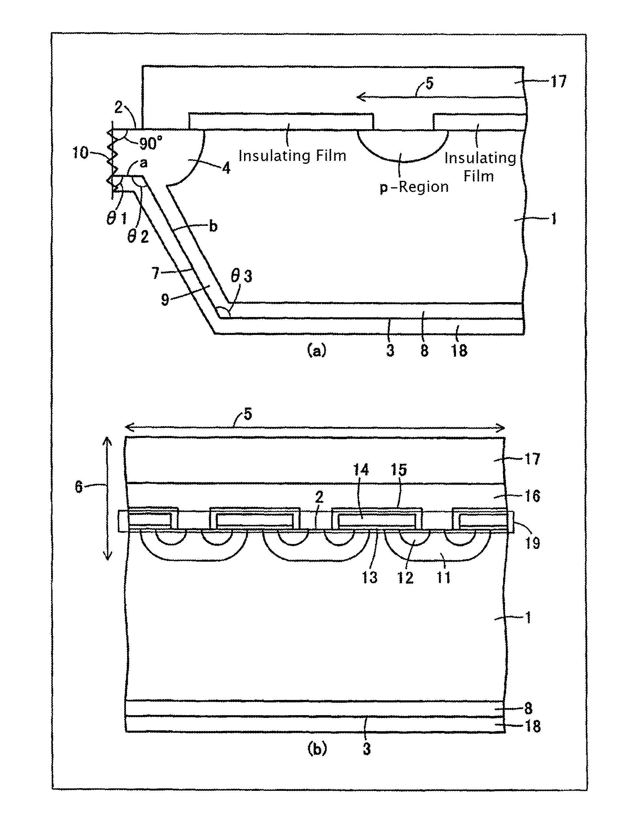
[0133]FIG. 1 is a cross-sectional view of a semiconductor device according to Example 1 of the present invention, where FIG. 1(a) is a cross-sectional view of a key portion near a p-isolation layer, and FIG. 1(b) is a cross-sectional view of a key portion of an active region. For this semiconductor device, a reverse blocking IGBT is described as an example. This reverse blocking IGBT comprises: an n-semiconductor substrate 1; a p-diffusion layer 4 which is formed on an outer periphery portion of the surface of a first principal plane 2 of the n-semiconductor substrate 1; a device surface structure 6 which is formed on a surface layer of an active region 5 (region where main current flows) of a first principal plane 2 (front face) of the n-semiconductor substrate 1 so as to be enclosed by the p-diffusion layer 4, isolated from the p-diffusion layer 4; a p-collector layer 8 which is formed on the surface layer of a second principal plane 3; a collector electrode 18 which is formed on ...

example 2

[0170]FIG. 12 is manufacturing process drawings depicting a method for manufacturing a semiconductor device of Example 2 of the present invention, where FIG. 12(a) is a plan view of the wafer, FIG. 12(b) is a cross-sectional view of a key portion sectioned at the X1-X1 line in FIG. 12(a), FIG. 12(c) is a cross-sectional view of a key portion sectioned at the X2-X2 line in FIG. 12(a), and FIG. 12(d) is a cross-sectional view of a key portion sectioned at the Y-Y line in FIG. 12(a). The dotted line in FIG. 12(d) indicates the thickness of the wafer 40 in a portion where the grooves 41 are not formed. FIG. 12 shows the processes of forming the grooves 41, in the case of the depth of the groove 41 is decreased in the outer periphery portion 44 of the wafer 40. The grooves 41 are formed all the way to the outer edge 45 of the wafer 40.

[0171]By forming the groove 41 to be shallower in the outer periphery portion 44 of the wafer 40, the film thickness of the residual film 43 becomes thicke...

example 3

[0172]FIG. 13 is manufacturing process drawings depicting a method for manufacturing a semiconductor device of Example 3 of the present invention, where FIG. 13(a) is a plan view of a process of a key portion of the wafer, and FIG. 13(b) is a cross-sectional view of a process of a key portion sectioned at the Y-Y line in FIG. 13(a). The dotted line in FIG. 13(b) indicates the thickness of the wafer 40 in a portion where the groove 41 is not formed. FIG. 13 shows the processes of forming the grooves 41, in the case where the depth of the groove 41 is decreased in an area away from the chip forming region 42, so that a part of the groove 41 does not reach the outer edge 45 of the wafer 40.

[0173]This makes the thickness of the residual film 43 in the outer periphery portion 44 thicker than the case of FIG. 12, so the wafer 40 is even less likely to be cracked than the case of FIG. 12. Further, an increase of the mechanical strength makes handling of the wager 40 even easier.


PUM


Abstract

Cutting work is performed on an n-semiconductor substrate (1) with an inverted trapezoid-shaped dicing blade to form grooves to be a second side walls (7). Bottom portions of the grooves are contacted with a p-diffusion layer (4) which is formed on a first principal plane (2) (front face) of the n-semiconductor substrate (1), so that the p-diffusion layer (4) is not cut. Then in the second side walls (7), a p-isolation layer (9) connected to a p-collector layer (8) and the p-diffusion layer (4) is formed. Since the p-diffusion layer (4) is not cut, a glass support substrate for supporting a wafer, and expensive adhesive, are not required, and therefore the p-isolation layer (4) can be formed at low cost.

Description

[0001]This application is a U.S. National Phase Application of PCT International Application PCT / JP2009 / 058927 filed on May 13, 2009 which is based on and claims priority from JP 2008-125402 filed on May 13, 2008 the contents of which are incorporated herein by reference in their entirety.TECHNICAL FIELD[0002]The present invention relates to a semiconductor device, such as a reverse blocking IGBT (Insulated Gate Bipolar Transistor) used for a power conversion device or the like, and a manufacturing method thereof.BACKGROUND ART[0003]A conventional method for manufacturing a reverse blocking IGBT will be described. A first prior art is a method of coating a dopant source and performing thermal diffusion from the surface of the dicing region on a wafer (silicon) in advance, before forming the gate / emitter structure constituting the reverse blocking IGBT, as shown in FIG. 26, where a deep p-isolation layer is formed, the wafer is thinned so that the p-isolation layer is exposed after t...

Claims


Application Information

Patent Timeline
Patent Type & Authority Patents(United States)
IPC IPC(8): H01L21/332
CPCH01L21/26586H01L21/268H01L21/67282H01L21/78H01L23/544H01L29/0657H01L29/7395H01L2924/0002H01L2223/54426H01L2223/5446H01L2924/00
Inventor TSUKAMOTO, YASUHIKOSHIMOYAMA, KAZUO
Owner FUJI ELECTRIC CO LTD
Why Eureka
Try Eureka