
Light-induced directed self-assembly of periodic sub-wavelength nanostructures

a sub-wavelength nanostructure and directed self-assembly technology, applied in the field of light-induced directed self-assembly of periodic sub-wavelength nanostructures, can solve the problems of low throughput of light, short-wavelength light source and associated optics, and inability to be readily available, etc., to achieve excellent long-range order, small feature size, and flexibility.

Active Publication Date: 2013-09-24
JUNIVERSITI OF NORT KAROLINA EHT SHARLOTT
View PDF16 Cites 1 Cited by
  • Summary
  • Abstract
  • Description
  • Claims
  • Application Information

AI Technical Summary

Benefits of technology

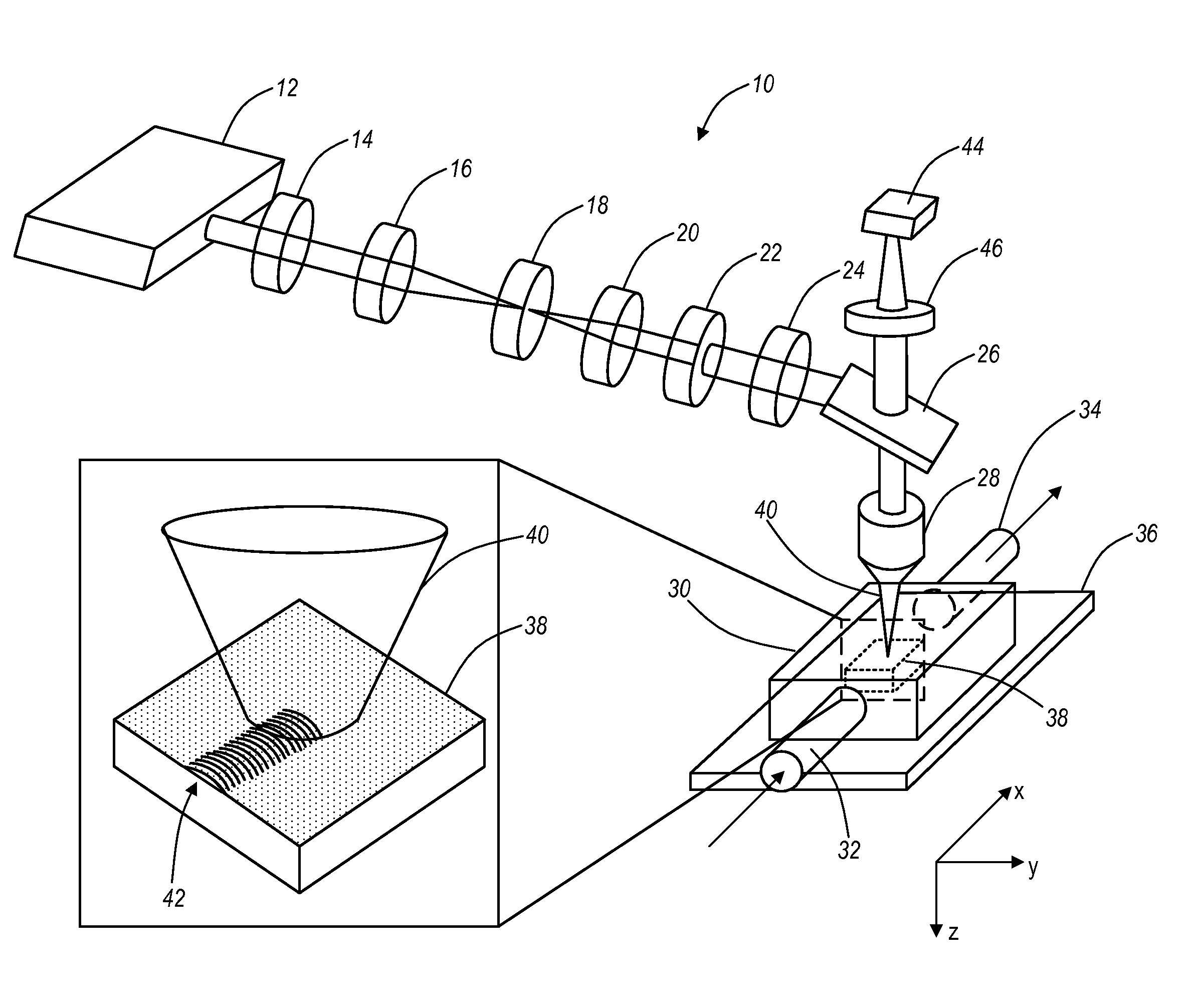
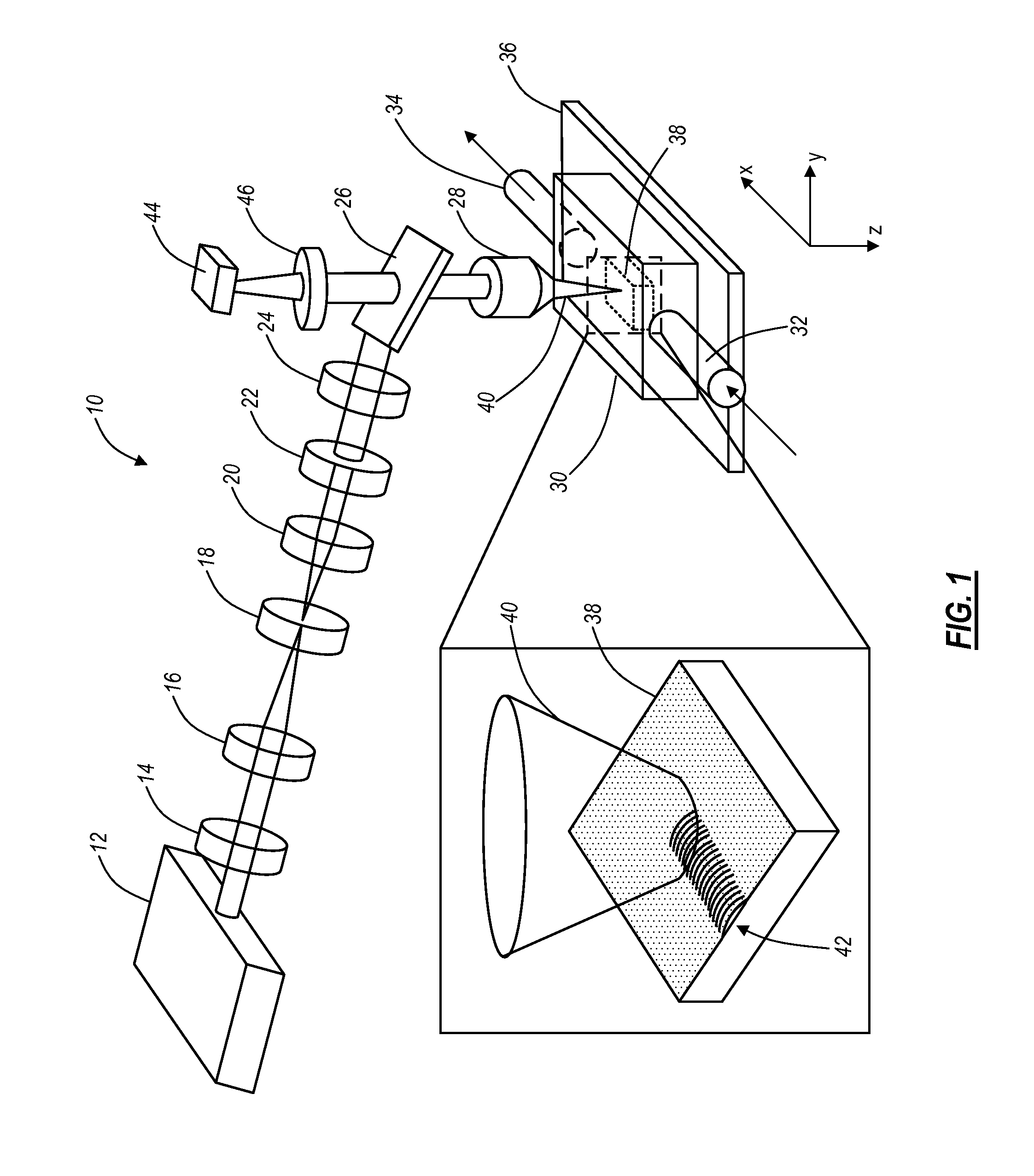
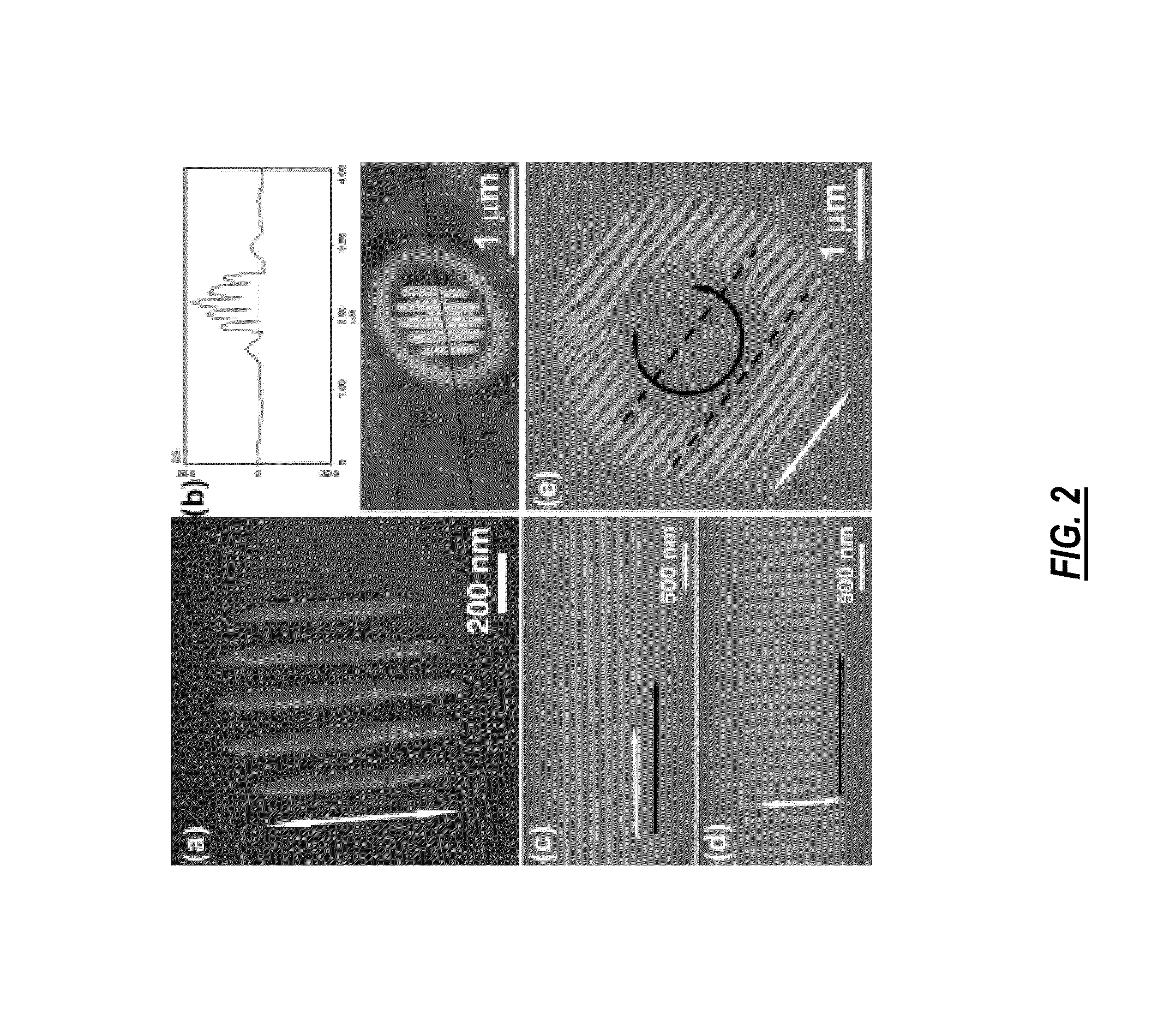
[0010]In various exemplary embodiments, the present invention provides a DW-LCVD technique that is capable of generating a feature size of λ / 5 or smaller, for example, processing multiple features simultaneously, and controlling the morphology of the deposited features, among other advantages. By gently focusing a single 400-nm 150-femtosecond laser beam or the like onto the surface of a substrate disposed in a vacuum chamber at or near room temperature with tungsten hexacarbonyl (W(CO)6) or the like as a precursor, the spontaneous formation of one-dimensional periodic or quasi-periodic nanostructures of tungsten or the like are grown heterogeneously on top of the underlying substrate without requiring any beam shaping, such masks or holography. The nanograting is formed simultaneously, and has a very small feature size. Metallic nanogratings with excellent long-range order are achieved simply by translating the substrate with respect to the laser focus. These metallic nanogratings may be formed on top of a variety of metals, semiconductors, and dielectrics, suggesting that the phenomenon of the present invention is a universal one. Considering the range of materials that may be deposited using DW-LCVD, the systems and methods of the present invention provide a simple, cost-effective, and flexible means to pattern periodic structures. Advantageously, micro and nanostructures, such as wires and spheres may be formed.

Problems solved by technology

However, due to their disruptive nature, these features may only be produced using amplified femtosecond pulses with a pulse energy that is at least a few hundred nanojoules or an intensity that is at least a few hundred terawatts per square centimeter.
However, the former suffers from low throughput of light, while the latter requires a short-wavelength light source and associated optics, which are not readily available.
This results in depositions with smooth profiles and limited morphological variations, such as lines, dots, or a combination of both.

Method used


Image

  • Light-induced directed self-assembly of periodic sub-wavelength nanostructures
  • Light-induced directed self-assembly of periodic sub-wavelength nanostructures
  • Light-induced directed self-assembly of periodic sub-wavelength nanostructures

Examples


Embodiment Construction

[0029]Again, in various exemplary embodiments, the present invention provides a DW-LCVD technique that is capable of generating a feature size of λ / 5 or smaller, for example, processing multiple features simultaneously, and controlling the morphology of the deposited features, among other advantages. By gently focusing a single 400-nm 150-femtosecond laser beam or the like onto the surface of a substrate disposed in a vacuum chamber at or near room temperature with tungsten hexacarbonyl (W(CO)6) or the like as a precursor, the spontaneous formation of one-dimensional grating-like nanostructures of tungsten or the like are grown heterogeneously on top of the underlying substrate without requiring any beam shaping, such masks or holography. The nanograting is formed simultaneously, and has a very small feature size. Metallic nanogratings with excellent long-range order are achieved simply by translating the substrate with respect to the laser focus. These metallic nanogratings may be ...


PUM

PropertyMeasurementUnit
wavelengthaaaaaaaaaa
diameteraaaaaaaaaa

Abstract

In various exemplary embodiments, the present invention provides a system for the light-induced directed self-assembly (LIDSA) of periodic sub-wavelength nanostructures, including: a light source for delivering a beam of photons; a reaction chamber disposed adjacent to the light source; a gas including one or more precursor materials disposed within the reaction chamber; and a substrate disposed within the reaction chamber, wherein the substrate is positioned and configured to receive the beam of photons; wherein the beam of photons causes a periodic sub-wavelength nanostructure of one or more constituents of the one or more precursor materials to form on a surface of the substrate. In various exemplary embodiments, the present invention also provides an associated method.

Description

CROSS-REFERENCE TO RELATED APPLICATION(S)[0001]The present non-provisional patent claims the benefit of priority of U.S. Provisional Patent Application No. 60 / 990,131, filed on Nov. 26, 2007, and entitled “TUNGSTEN NANOSTRUCTURES,” the contents of which are incorporated in full by reference herein.STATEMENT REGARDING FEDERALLY-SPONSORED RESEARCH OR DEVELOPMENT[0002]The U.S. Government has a paid-up license in the present invention and the right, in limited circumstances, to require the patent owner to license to others on reasonable terms as provided for by the terms of Contract No. W911NF-05-2-0053 awarded by the Defense Advanced Research Projects Agency (DARPA).FIELD OF THE INVENTION[0003]The present invention relates generally to the light-induced directed self-assembly (LIDSA) of periodic sub-wavelength nanostructures. More specifically, the present invention relates to systems and methods for fabricating periodic sub-wavelength nanostructures using laser chemical vapor depositi...

Claims


Application Information

Patent Timeline
Patent Type & Authority Patents(United States)
IPC IPC(8): C08J7/18
CPCG11B7/0045G11B7/0065C23C16/483C23C16/047C23C16/16B82Y10/00G11B7/083Y10T428/12G11B2007/13727Y10T428/31678
Inventor HER, TSING-HUAZHANG, HAITAOTANG, MINGZHEN
Owner JUNIVERSITI OF NORT KAROLINA EHT SHARLOTT
Learn More