

Method for manufacturing semiconductor device
a semiconductor and manufacturing method technology, applied in the direction of semiconductor devices, basic electric elements, electrical appliances, etc., can solve the problems of increasing the threshold voltage of transistors, reducing the density of states attributed to oxygen vacancy in the oxide semiconductor layer, and increasing the thickness of the oxide semiconductor layer
- Summary
- Abstract
- Description
- Claims
- Application Information
AI Technical Summary
Benefits of technology
Problems solved by technology
Method used
Image

Examples
embodiment 1
(Embodiment 1)
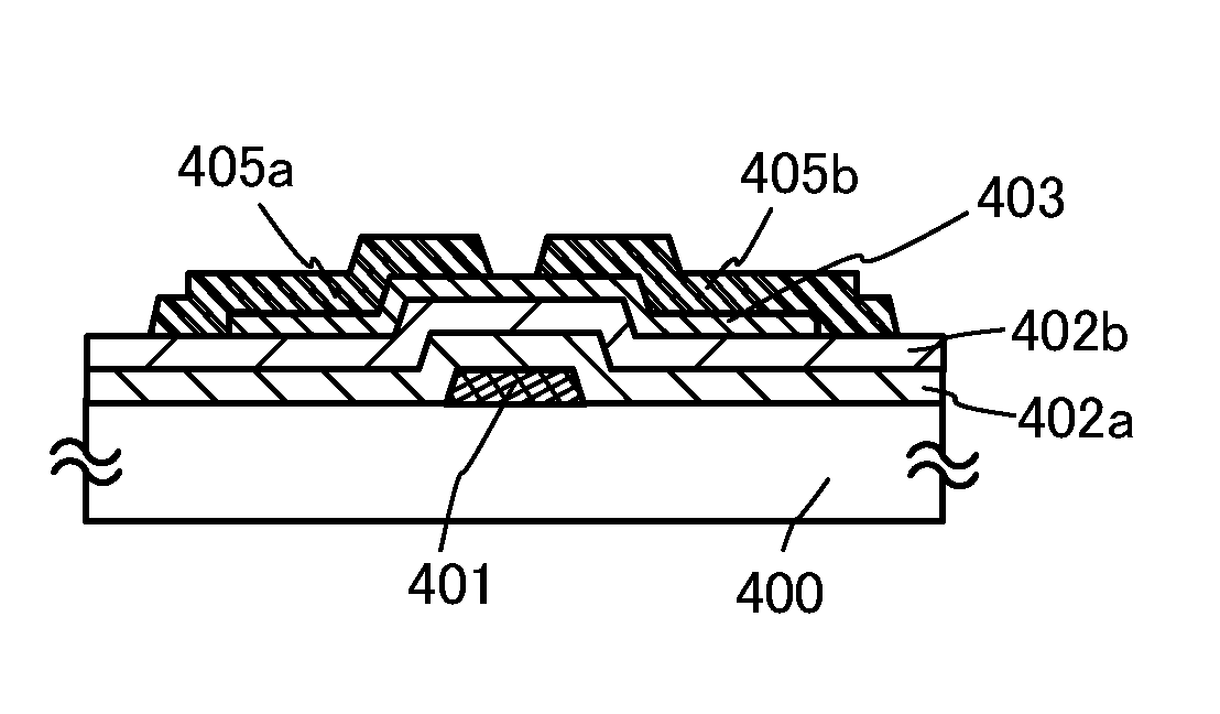
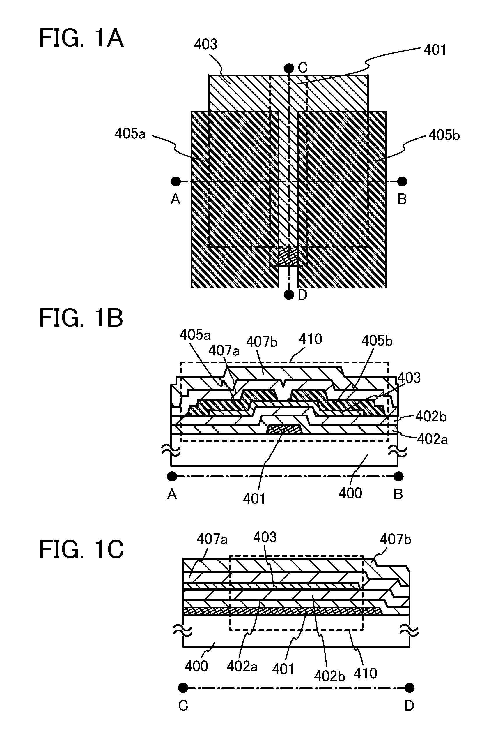
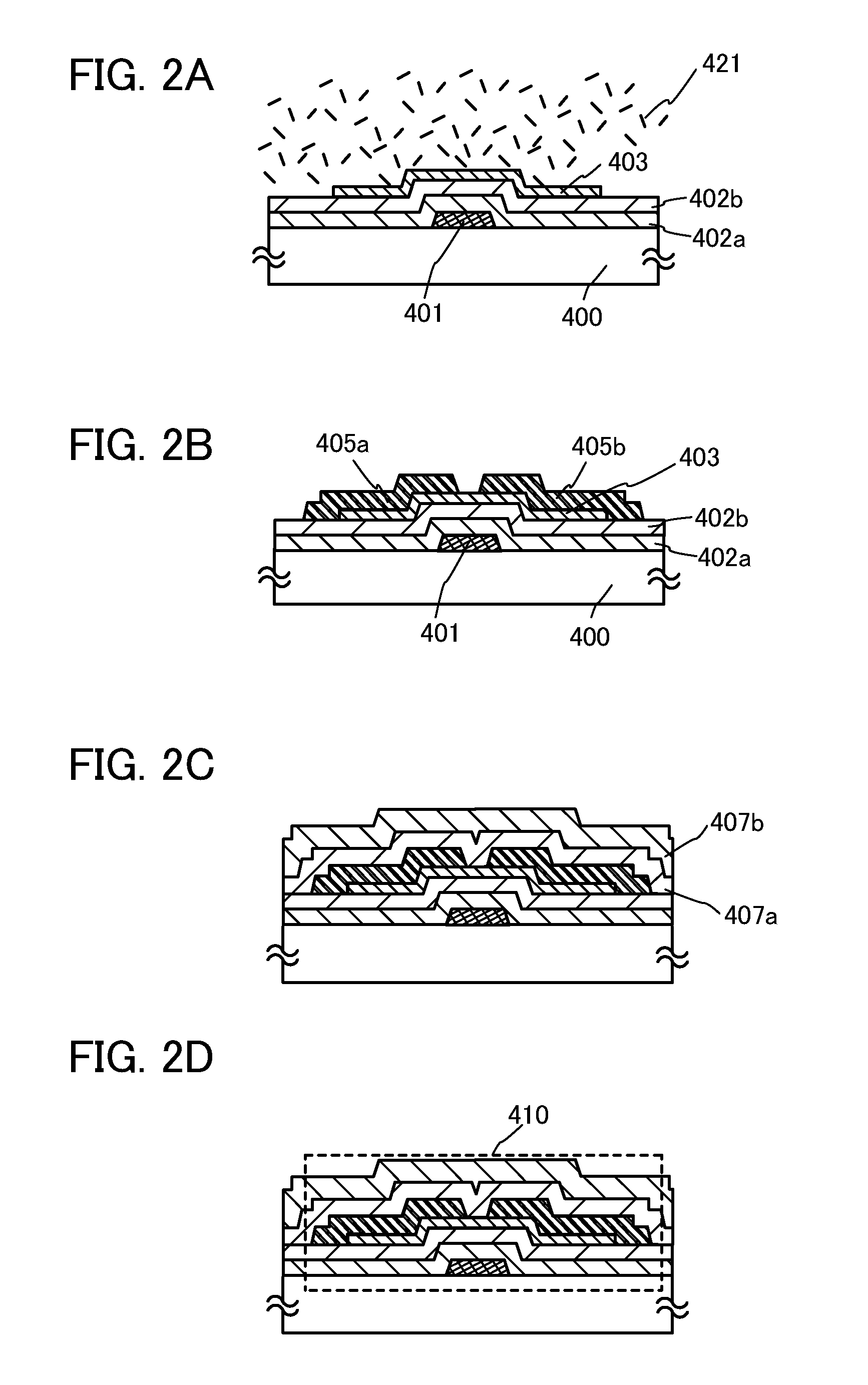
[0043]In this embodiment, one embodiment of a semiconductor device and a method for manufacturing the semiconductor device will be described with reference to FIGS. 1A to 1C, FIGS. 2A to 2C, and FIGS. 3A to 3C. In this embodiment, a transistor including an oxide semiconductor layer is shown as an example of the semiconductor device.
[0044]FIGS. 1A to 1C are a plan view and cross-sectional views of a bottom-gate transistor 410 as an example of a semiconductor device. FIG. 1A is a plan view and FIGS. 1B and 1C are cross-sectional views taken along line A-B and line C-D in FIG. 1A, respectively. Note that some components of the transistor 410 (e.g., a silicon oxide film 407a, an aluminum oxide film 407b, and the like) are not illustrated in FIG. 1A in order to avoid complexity.
[0045]The transistor 410 illustrated in FIGS. 1A to 1C includes, over a substrate 400 having an insulating surface, a gate electrode layer 401, an aluminum oxide film 402a and a silicon oxide film 40...
embodiment 2
(Embodiment 2)
[0109]In this embodiment, an example of a deposition apparatus for forming an oxide semiconductor layer and the like in the semiconductor device described in Embodiment 1 will be described with reference to FIGS. 4A to 4C, FIGS. 5A to 5C, and FIGS. 6A and 6B. Note that the same portion as or a portion having a function similar to that in Embodiment 1 can be formed as in Embodiment 1, and the same step as or a step similar to that in Embodiment 1 can be performed as in Embodiment 1, and thus repetitive description is omitted. In addition, detailed description of the same portion is not repeated.
[0110]FIG. 4A is a block diagram illustrating a structure of a deposition apparatus described in this embodiment.
[0111]In the deposition apparatus, a load chamber 101, a first deposition chamber 111, a second deposition chamber 112, a third deposition chamber 113, a heating chamber 114, an oxygen-supplying treatment chamber 115, and an unload chamber 102 are connected in this ord...
embodiment 3
(Embodiment 3)
[0163]A semiconductor device having a display function (also referred to as display device) can be manufactured using the transistor described in Embodiment 1. Moreover, some or all of driver circuits which include transistors can be formed over a substrate where a pixel portion is formed, whereby a system-on-panel can be obtained.
[0164]In FIG. 8A, a sealant 4005 is provided so as to surround a pixel portion 4002 provided over a first substrate 4001, and the pixel portion 4002 is sealed by the sealant 4005 and a second substrate 4006. In FIG. 8A, a signal line driver circuit 4003 and a scan line driver circuit 4004 which are each formed using a single crystal semiconductor film or a polycrystalline semiconductor film over a substrate prepared separately are mounted in regions that are different from the region surrounded by the sealant 4005 over the first substrate 4001. Various signals and potentials are supplied to the signal line driver circuit 4003, the scan line d...
PUM
| Property | Measurement | Unit |
|---|---|---|
| temperature | aaaaa | aaaaa |
| thickness | aaaaa | aaaaa |
| thickness | aaaaa | aaaaa |
Abstract
Description
Claims
Application Information