

Process for production of silicon single crystal, and highly doped N-type semiconductor substrate
a production method and semiconductor technology, applied in the direction of polycrystalline material growth, conductors, under protective fluids, etc., can solve the problems of abnormal growth (cell growth) and compound supercooling phenomenon
- Summary
- Abstract
- Description
- Claims
- Application Information
AI Technical Summary
Benefits of technology
Problems solved by technology
Method used
Image

Examples
Embodiment Construction
[0042]An exemplary embodiment of the invention will be described below with reference to the attached drawings.
[0043]1. On Abnormal Growth
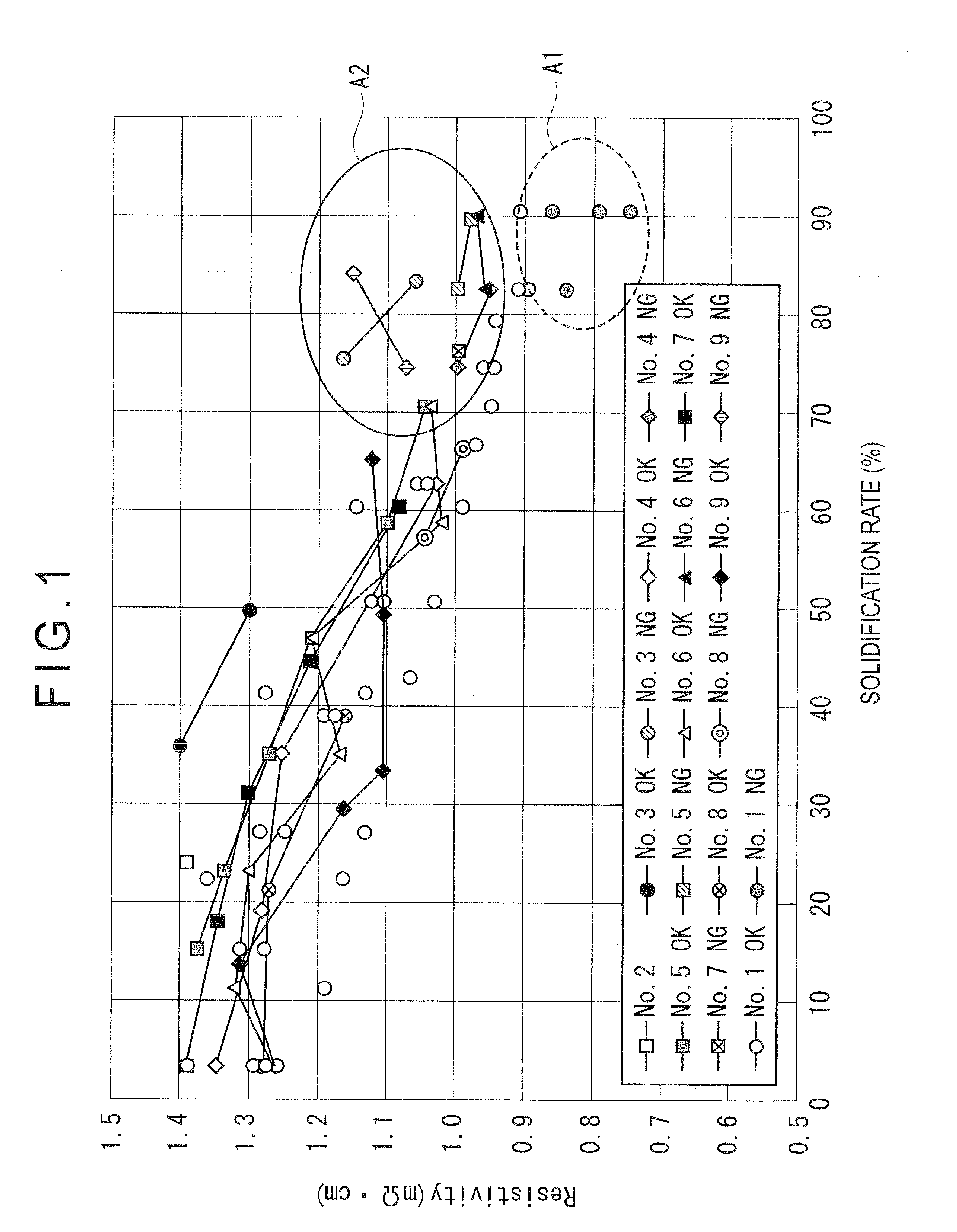
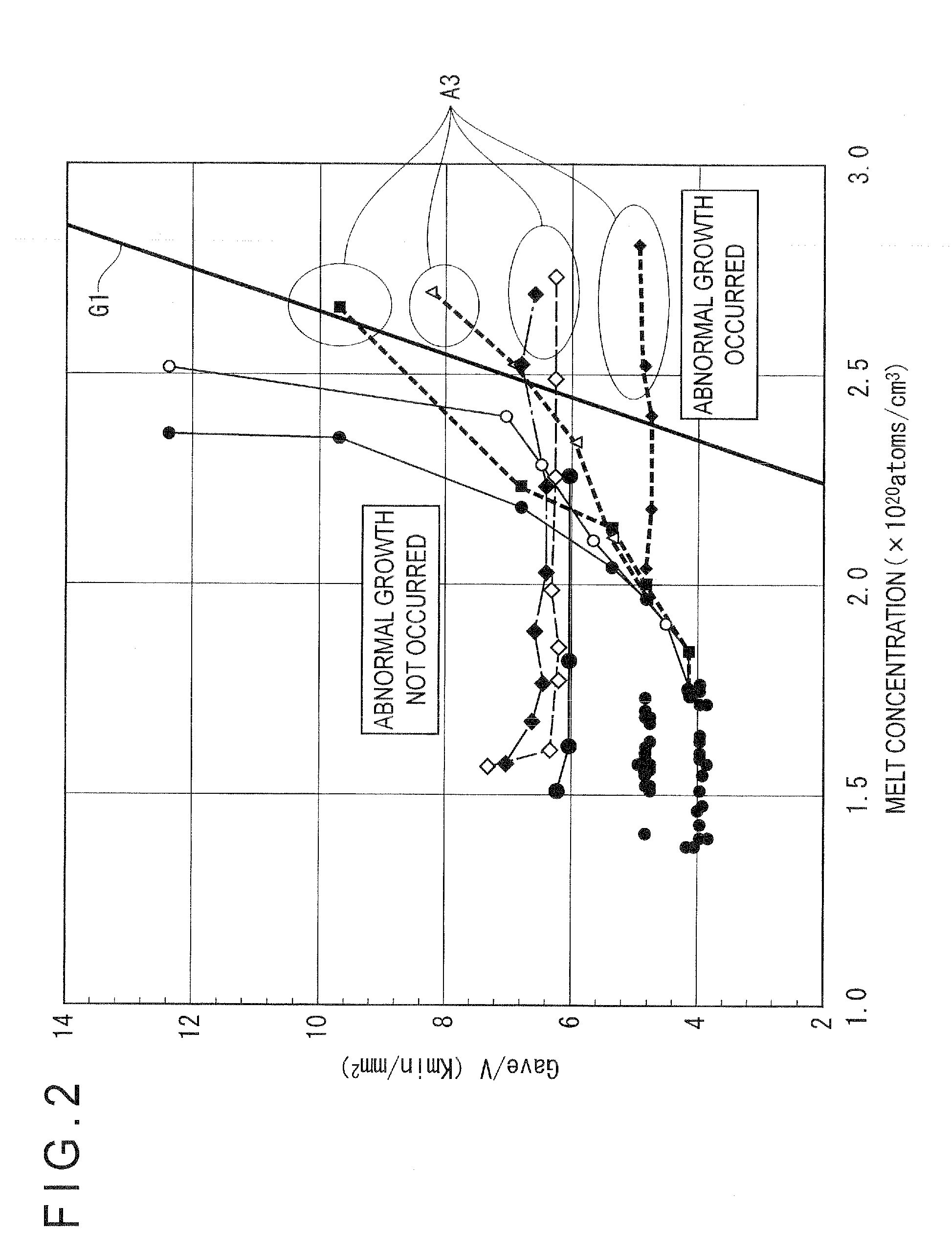
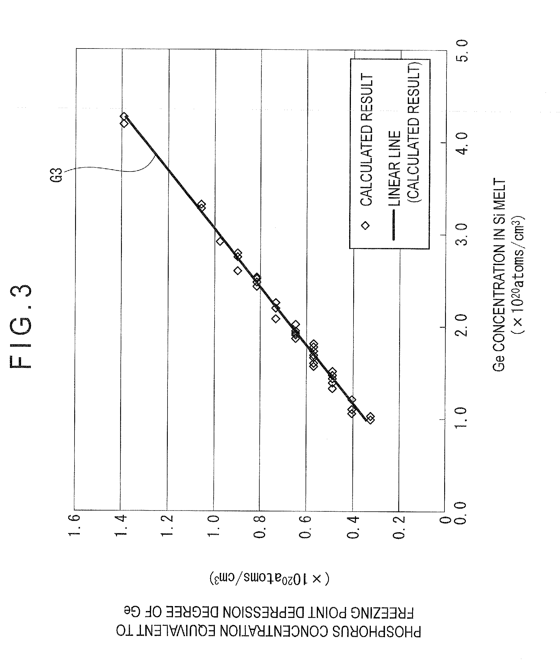
[0044]Initially, abnormal growths occurred when a monocrystal is grown by CZ method from a silicon melt in which only phosphorus is doped and from a silicon melt in which phosphorus and germanium are co-doped are checked. Pull-up conditions at this time are shown in the following tables 1 and 2, where a pull-up speed as well as a doping amount of germanium is altered as a control parameter.
[0045]Incidentally, in order to co-dope phosphorus and germanium, the following arrangement is employed.
[0046]Initially, a doping device having an upper dopant chamber and a lower dopant chamber are provided, the upper and lower dopant chambers respectively accommodating different dopants, an upper part of the upper dopant chamber being opened and a lower part of the lower dopant chamber being opened. Phosphorus is accommodated in the upper dopant chamber and ge...
PUM
| Property | Measurement | Unit |
|---|---|---|
| resistivity | aaaaa | aaaaa |
| resistivity | aaaaa | aaaaa |
| resistivity | aaaaa | aaaaa |
Abstract
Description
Claims
Application Information