

Method of forming patterns
a pattern and pattern technology, applied in the field of pattern formation, can solve the problems of resist layer degradation, resist description suitable for immersion lithography, and reduction in exposure speed, and achieve the effect of enhancing in-plane uniformity of line width and reducing line edge roughness
- Summary
- Abstract
- Description
- Claims
- Application Information
AI Technical Summary
Benefits of technology
Problems solved by technology
Method used
Image

Examples
synthesis example 1
Synthesis of Resin (D20))
[0595]In propylene glycol monomethyl ether acetate, 47.2 g of hexafluoroisopropyl acrylate (a product of Wako Pure Chemical Industries, Ltd.) is dissolved, thereby preparing 170 g of a solution having a solid concentration of 20%. To this solution, 8 mole % (3.68 g) of a polymerization initiator V-601 (a product of Wako Pure Chemical Industries, Ltd.) is added. In an atmosphere of nitrogen, the resultant solution is added dropwise over 4 hours to 20.0 g of propylene glycol monomethyl ether acetate heated to 80° C. After the conclusion of dropwise addition, the reaction solution is stirred for 2 hours, thereby obtaining a Reaction Solution (1). After the completion of the reaction, the Reaction Solution (1) is cooled to room temperature, and then added dropwise to a twenty-times greater amount of 8:1 methanol-water solvent mixture. An oily compound thus separated is collected by decantation to yield 24.1 g of the intended Resin (D20).
[0596]The weight average ...
synthesis example 2
Synthesis of Resin (A1)
[0599]In a stream of nitrogen, 20 g of 6:4 (by mass) solvent mixture of propylene glycol monomethyl ether acetate and propylene glycol monomethyl ether is put in a three-necked flask and heated up to 80° C. (Solvent 1). A monomer mixture composed of γ-butyrolactone methacrylate, hydroxyadamantane methacrylate and 2-methyl-2-adamantyl methacrylate in proportions of 40:25:35 by mole is added to a 6:4 (by mass) solvent mixture of propylene glycol monomethyl ether acetate and propylene glycol monomethyl ether, thereby preparing a 22 mass % monomer solution (200 g). Further, an initiator V-601 (a product of Wako Pure Chemical Industries, Ltd.) is added to and dissolved in the monomer solution in an amount of 8 mole % based on the total monomers. The resultant solution is added dropwise to the Solvent 1 over 6 hours. After the conclusion of dropwise addition, reaction is made to continue at 80° C. for additional 2 hours. The reaction solution obtained is allowed to ...
example 1
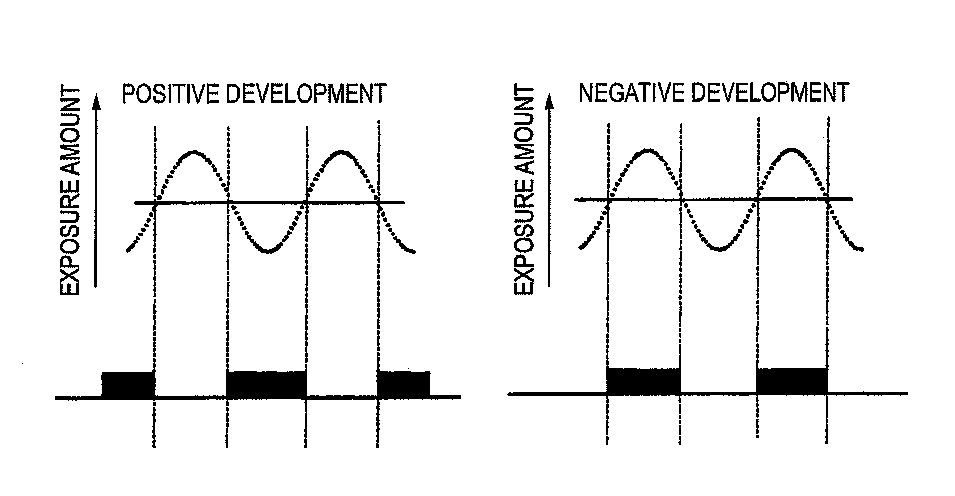
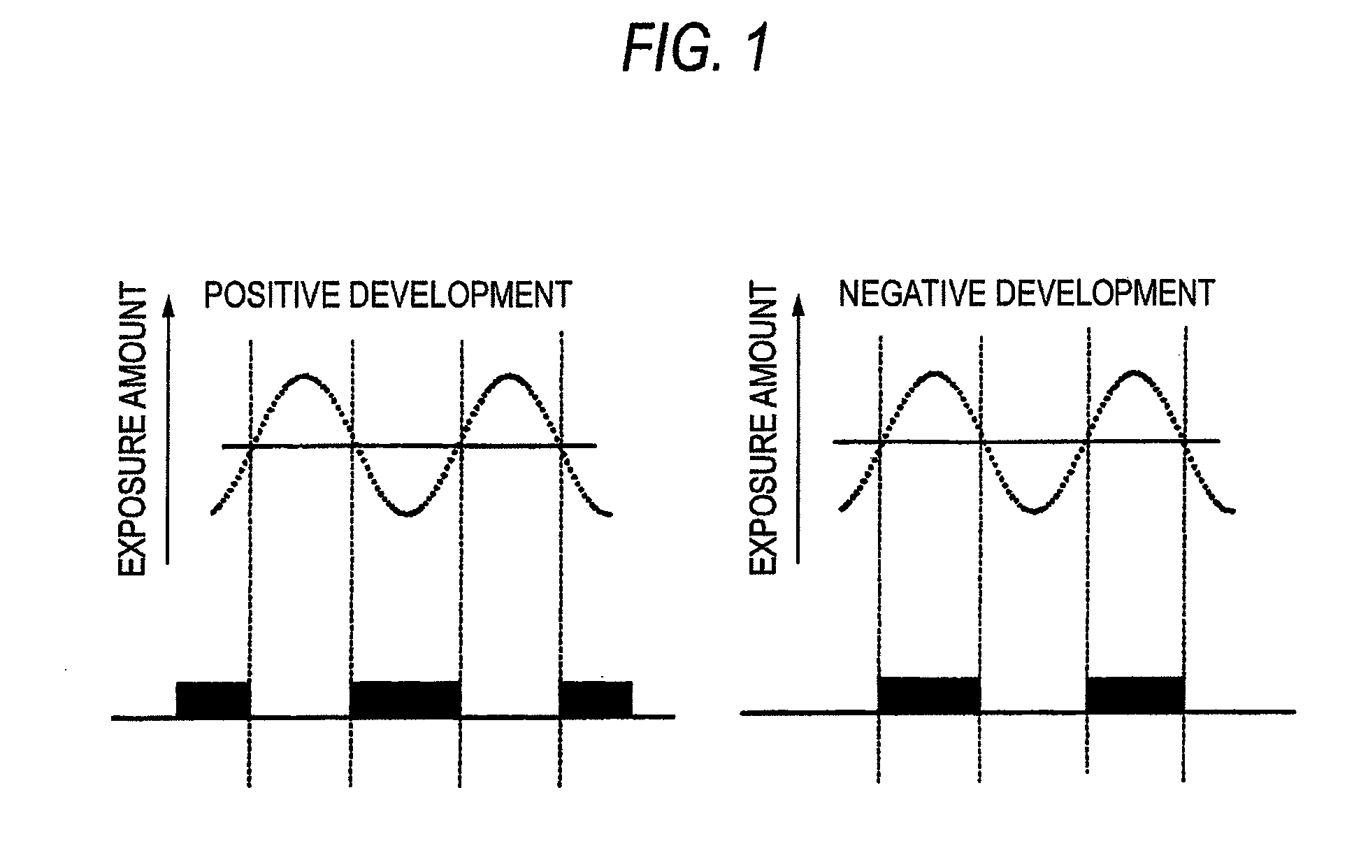
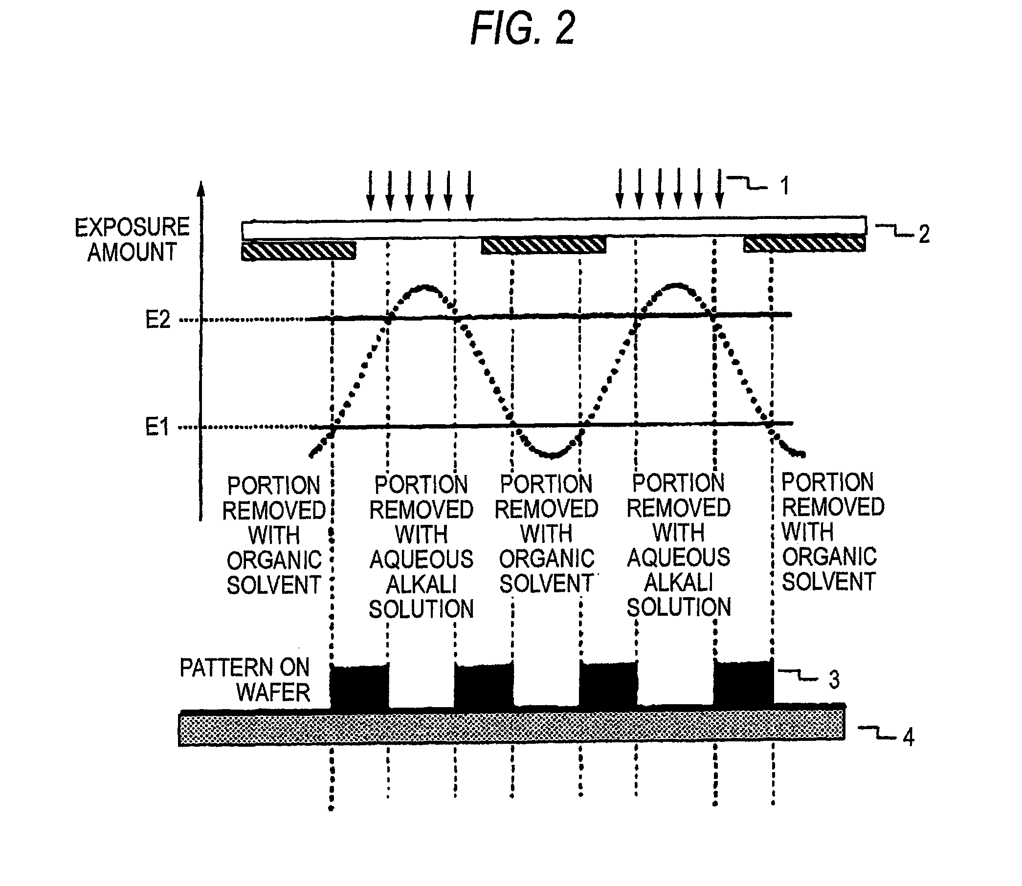
Negative Development
[0608]An organic antireflective film ARC29A (a product of Nissan Chemical Industries, Ltd.) is applied to a silicon wafer surface, and baked at 205° C. for 60 seconds, thereby forming a 78 nm-thick antireflective film. On this film, the resist composition Ra1 is spin-coated, and baked at 120° C. for 60 seconds, thereby forming a 150 nm-thick resist film. The thus obtained wafer is subjected to immersion exposure via a mask for pattern formation, wherein purified water is used as the immersion liquid and PAS5500 / 1250i equipped with a lens of NA=0.85 (made by ASML) is used as an ArF excimer laser scanner. After the exposure, the wafer is spun at revs of 2,000 rpm, and thereby the water remaining on the wafer is removed. Then, the wafer is subjected successively to 60 seconds' heating at 120° C., 60 seconds' development (negative development) with butyl acetate (negative developer), rinse with 1-hexanol, and 30 seconds' spinning at revs of 4,000 rpm. Thus, 80-nm (1:...
PUM
| Property | Measurement | Unit |
|---|---|---|
| receding contact angle | aaaaa | aaaaa |
| vapor pressure | aaaaa | aaaaa |
| wavelength | aaaaa | aaaaa |
Abstract
Description
Claims
Application Information