Method of making a nanostructure

a nanostructure and nano-technology, applied in the field of nanostructure making, can solve the problems of limited commercial viability of the method, limited anti-reflective regions on the substrate, complicated batch process, etc., and achieve the effect of reducing reflectance and scratch resistan

Active Publication Date: 2014-01-21
3M INNOVATIVE PROPERTIES CO
View PDF28 Cites 58 Cited by
  • Summary
  • Abstract
  • Description
  • Claims
  • Application Information

AI Technical Summary

Benefits of technology

[0014]The nanostructured surfaces prepared by the provided method can exhibit a significant reduction in reflectance compared to an unstructured surface comprising the same materials. In addition, the nanostructured articles can be durable and possess scratch resistance. The provided method can be carried out at

Problems solved by technology

Known methods for creating the subwavelength surface structure tend to be complicated and expensive batch processes, however.
This requirement of extreme vacuum cond

Method used


Image

  • Method of making a nanostructure
  • Method of making a nanostructure
  • Method of making a nanostructure

Examples


examples

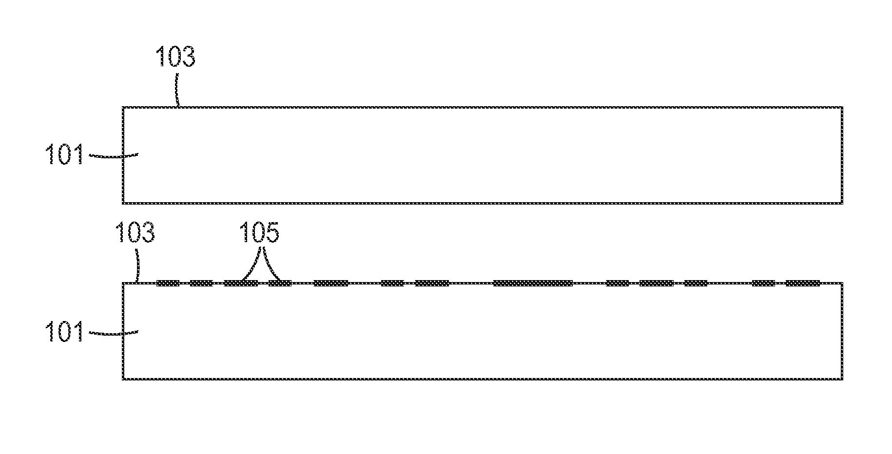
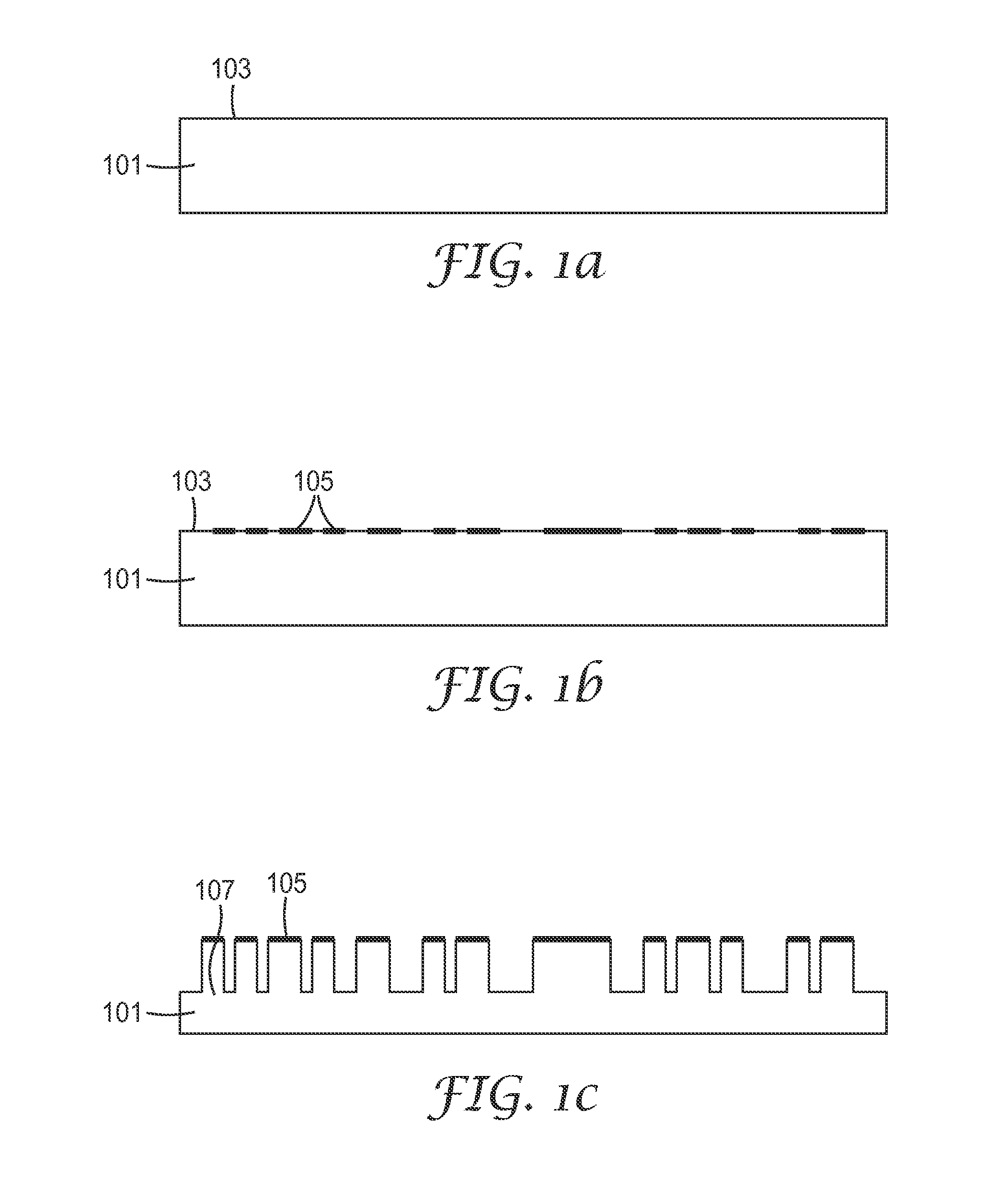
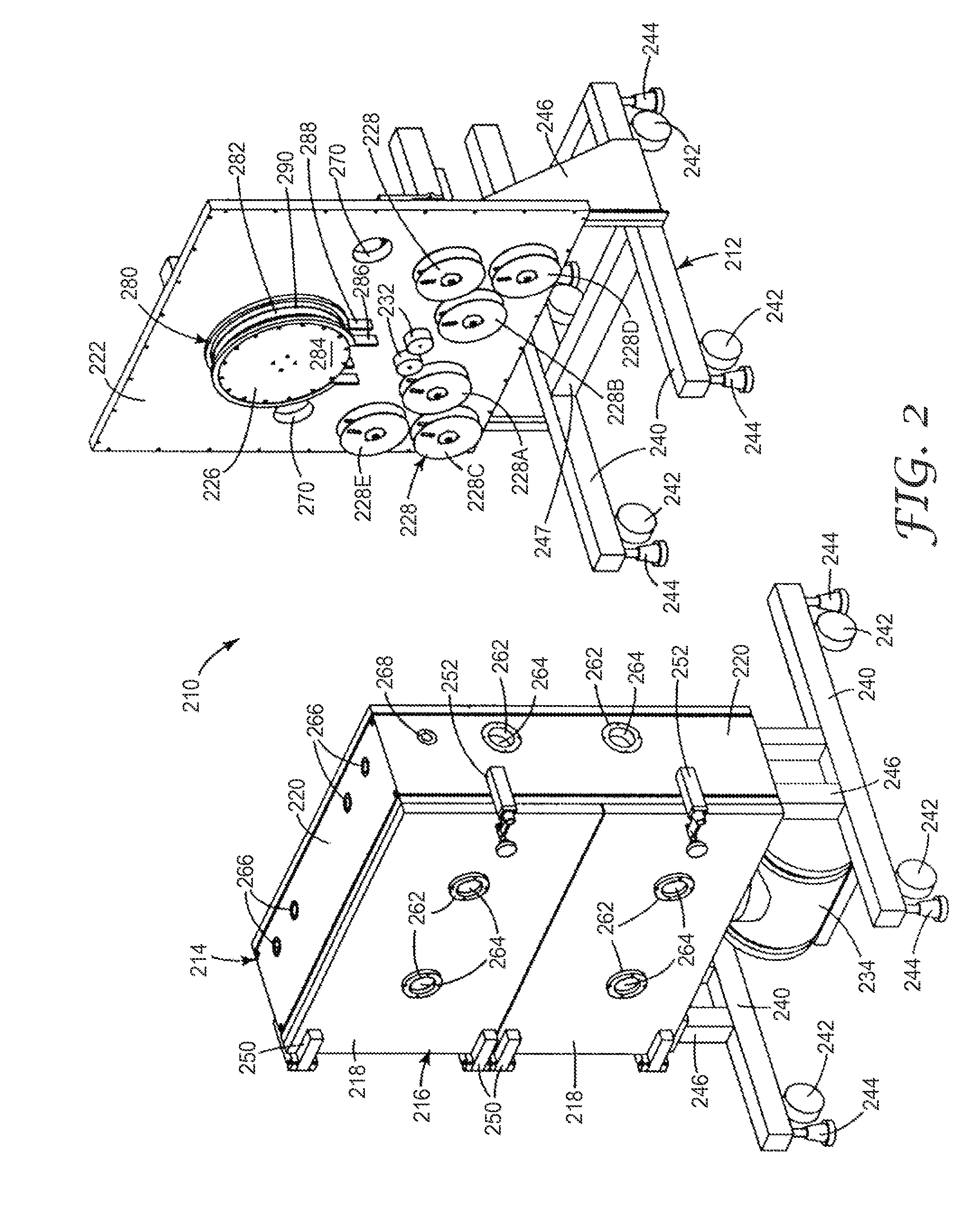
[0072]The provided nanostructures and methods described herein were obtained by using a homebuilt plasma treatment system described in detail in U.S. Pat. No. 5,888,594 (David et al.) with some modifications and is illustrate in FIGS. 2, 3, and 4ab. The width of the drum electrode was increased to 14.5 inches (36.8 cm) and the separation between the two compartments within the plasma system was removed so that all the pumping was carried out by means of the turbo-molecular pump and thus operating at a much lower operating pressure than is conventionally done with plasma processing.

[0073]Rolls of polymeric film were mounted within the chamber, the film wrapped around the drum electrode and secured to the take up roll on the opposite side of the drum. The unwind and take-up tensions were maintained at 3 pounds (13.3 N). The chamber door was closed and the chamber pumped down to a base pressure of 5×10⁻⁴ torr. For the deposition of an discontinuous mask layer, tetramethylsilane gas at ...

examples 1-8

Nanostructure Formed on PMMA Substrate Film

[0077]PMMA film sheets were first exposed to a tetramethylsilane (TMS) plasma at a web speed of either 7.5 feet / min (2.3 m / min) or 8.5 feet / min (2.6 m / min) and the oxygen etching was carried out for four different, 30, 60, 90 and 120 seconds. The resulting sheet articles demonstrated outstanding average % transmission and anti-reflection (average % reflection) properties as summarized in Table 1 below:

[0078]

TABLE 1Optical Properties of Nanostructured PMMA films (Examples 1-8)% RTMS / ARRIEExam-% R (without(tapedepositionEtchingpletape correct)correct)% T% H(m / min)Time12.431.8596.12.382.612021.330.7697.11.362.69031.360.7897.20.742.66042.441.8796.30.482.63051.130.5696.52.152.312060.980.4196.71.622.39071.220.6497.30.742.36084.323.7595.80.592.330

The optical reflectance spectra of these films are summarized in FIG. 5, where the broad-band anti-reflection performance is displayed.

[0079]The surface morphology of the PMMA films of was determined by S...


PUM

PropertyMeasurementUnit
Nanoscale particle sizeaaaaaaaaaa

Abstract

A method of making a nanostructure is provided that includes applying a thin, random discontinuous masking layer (105) to a major surface (103) of a substrate (101) by plasma chemical vapor deposition. The substrate (101) can be a polymer, an inorganic material, an alloy, or a solid solution. The masking layer (105) can include the reaction product of plasma chemical vapor deposition using a reactant gas comprising a compound selected from the group consisting of organosilicon compounds, metal alkyls, metal isopropoxides, metal acetylacetonates, and metal halides. Portions (107) of the substrate (101) not protected by the masking layer (105) are then etched away by reactive ion etching to make the nanostructures.

Description

FIELD[0001]A method is provided for making nanostructures on surfaces.BACKGROUND[0002]Nanostructures have been found to impart useful properties on surfaces of articles. These useful properties include useful optical properties, such as, for example, reflection reduction of plastic substrates, useful mechanical properties, such as, for example, surface modification for improved adhesion, and for creating features on surfaces that can be useful in, for example, drug delivery.[0003]Many methods exist to generate nanostructure on surfaces of articles. For example, plasma etching is a useful method that has been used to generate nanostructures. A type of plasma etching, reactive ion etching (RIE), has been widely employed in the semiconductor industry to produce submicron features useful in electronics. However, when the feature sizes reach below about 200 micrometers, charging effects of the surface features prevent pattern transfer of features having high aspect ratios. Recently, high...

Claims


Application Information

Patent Timeline
IPC IPC(8): C23C14/28G02B3/08
CPCB82Y40/00B82Y30/00B82Y20/00B29C2059/023G02B1/118B29C59/14C23C16/04Y10T428/24479C23C16/56C23F1/02G02B3/08
Inventor DAVID, MOSES M.YU, TA-HUAHARTZELL, ANDREW K.
Owner 3M INNOVATIVE PROPERTIES CO
Why Eureka
Try Eureka