Magnetic tunnel junction for MRAM applications

a magnetic tunnel junction and mram technology, applied in galvano-magnetic devices, solid-state devices, instruments, etc., can solve the problems of disadvantage, cofeb has a relatively high magnetoresistance value, and the other parameter degradation, so as to improve the bit switching characteristic of a mram

Active Publication Date: 2014-07-22
TAIWAN SEMICON MFG CO LTD
View PDF20 Cites 13 Cited by
  • Summary
  • Abstract
  • Description
  • Claims
  • Application Information

AI Technical Summary

Benefits of technology

[0013]One objective of the present invention is to provide an improved MTJ element that enhances the bit switching characteristic of a MRAM such that the number of unswitched bits at a given bit line current is reduced compared with the prior art.
[0015]A third objective of the present invention is to simultaneously achieve a reduced number of shorted bits and enhanced bit switching property including a lower switching current without degrading the MR ratio of the MTJ.
[0016]According to a first embodiment, these objectives are achieved with a MTJ element comprised of at least a pinned layer / tunnel barrier layer / free layer configuration wherein a composite free layer adjoins a surface of the tunnel barrier layer which is preferably MgO. A key feature is the composite free layer that has a crystalline ferromagnetic layer adjoining the tunnel barrier layer and an amorphous layer contacting an opposing surface of the crystalline layer with respect to the MgO / crystalline layer interface. In particular, the crystalline layer preferably has a (001) bcc structure that leads to a high TMR ratio while the amorphous layer improves bit switching and bit shorting characteristics. For example, a Fe / NiFeHf composite free layer is especially suited to realize the objectives and advantages of the present invention. However, the NiFeHf layer should be in the range of 20 to 40 Angstroms thick to provide the full advantage of a reduced number of shorted bits and a substantially lower bit switching current. In an alternative embodiment, Hf may be replaced by X=Mg, Ta, Zr, or Nb. Preferably, the NiFeX layer has a sufficiently high X content to provide an amorphous structure.

Problems solved by technology

Typically, an improvement in one property leads to a degradation in one or more other parameters.
However, CoFeB is known to have a relatively high magnetoresistance value which is a disadvantage.

Method used


Image

  • Magnetic tunnel junction for MRAM applications
  • Magnetic tunnel junction for MRAM applications
  • Magnetic tunnel junction for MRAM applications

Examples


first embodiment

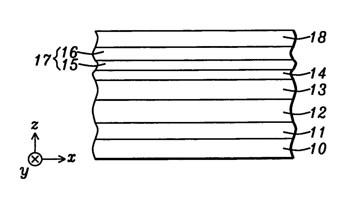
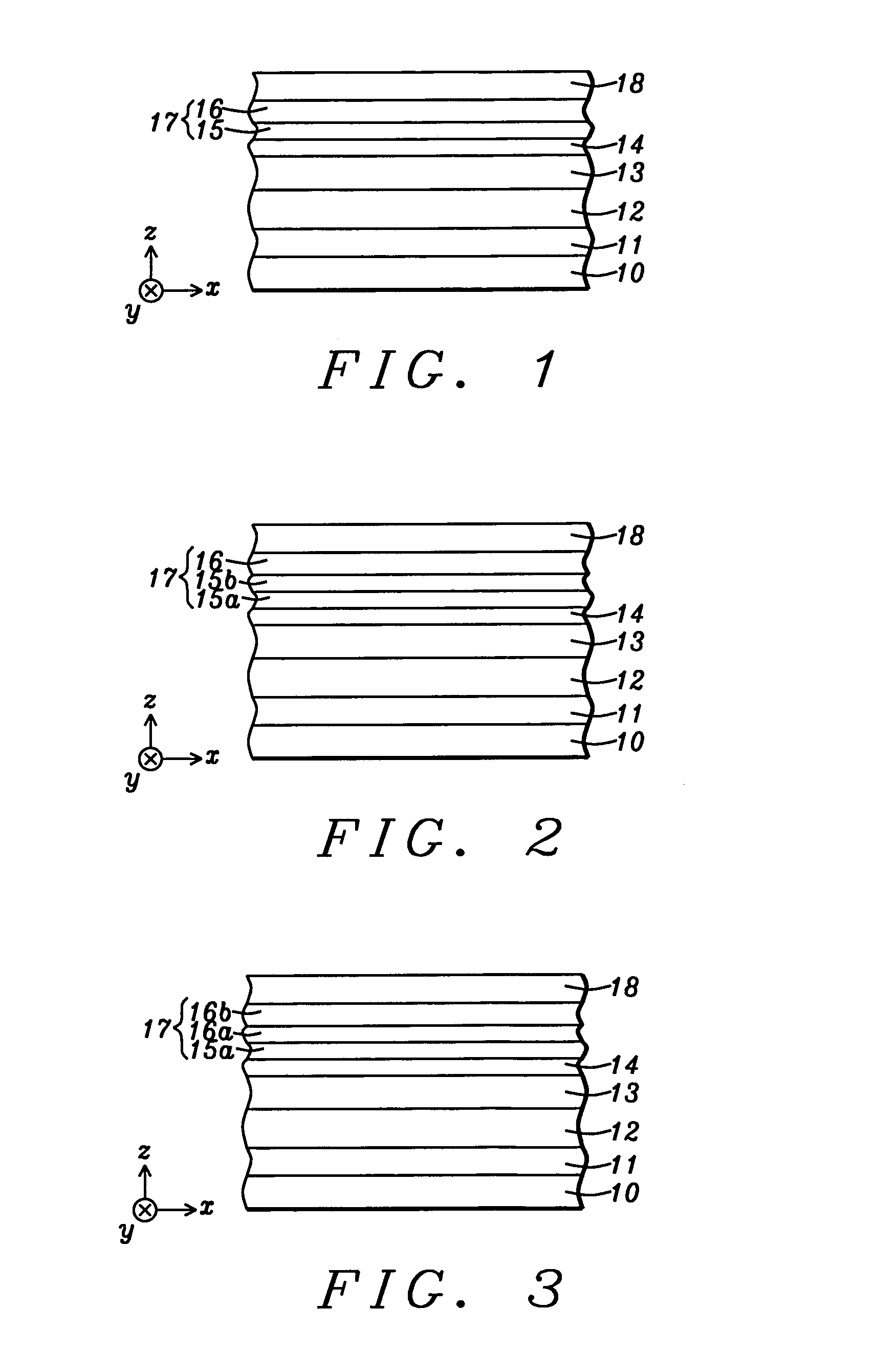
[0026]Referring to FIG. 1, a MTJ structure is illustrated according to the present invention. The substrate 10 may be a bottom conductor layer, for example, having a thickness in the z-axis direction and with a top surface in the x,y plane. A MTJ stack of layers is now formed on the substrate 10. It should be understood that all layers in the MTJ stack may be formed in the same process tool such as an Anelva C-7100 thin film sputtering system or the like which typically includes three physical vapor deposition (PVD) chambers each having 5 targets, an oxidation chamber, and a sputter etching chamber. At least one of the PVD chambers is capable of co-sputtering. Typically, the sputter deposition process involves an argon sputter gas and the targets are made of metal or alloys to be deposited on a substrate. All MTJ layers may be formed after a single pump down of the sputter system to enhance throughput.

[0027]In the exemplary embodiment, the MTJ stack of layers is fabricated on the su...

embodiment 2

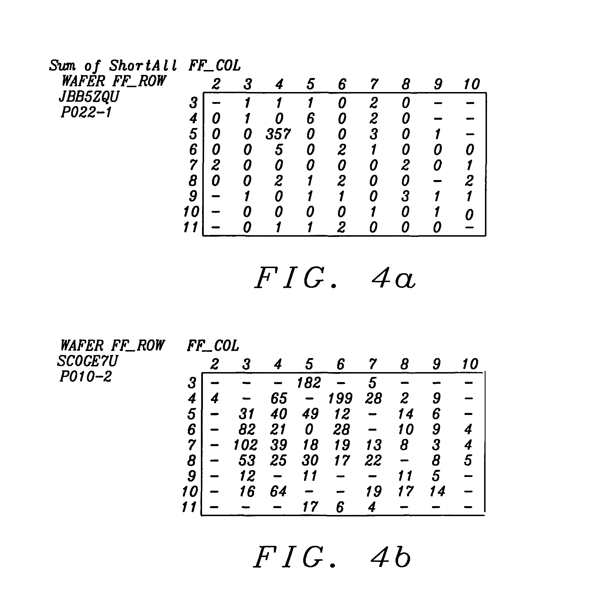
[0043]In all examples except reference 2, a NiRFeSHfT layer where R=75, S=10, and T=15 was deposited by co-sputtering a NiRFeS target and a Hf target in an Anelva 7100 sputter deposition system. With regard to the example representing embodiment 2, the NiFe layer has a Ni content of 88 atomic %. References 1-3 include free layer stacks previously built by the inventors for other experiments. TMR ratios for the examples representing embodiments 1 and 2 demonstrate that dR / R is as high as the value in other designs such as reference 1. One advantage of the present invention as found in the embodiments described herein is a dramatic reduction in the number of shorted bits in MRAM devices.

[0044]Referring to FIG. 4, the MTJs of Embodiment 1 and Reference 1 above were incorporated in 4 Mb MRAM chips. The table in FIG. 4 shows the number of shorted bits per 0.5 Mb section of a 4 Mb chip, measured for multiple chips across an 8 inch wafer. Each number shown by column and row corresponds to ...


PUM

PropertyMeasurementUnit
thicknessaaaaaaaaaa
thicknessaaaaaaaaaa
thicknessaaaaaaaaaa

Abstract

A MTJ in an MRAM array is disclosed with a composite free layer having a lower crystalline layer contacting a tunnel barrier and an upper amorphous NiFeX layer for improved bit switching performance. The crystalline layer is Fe, Ni, or FEB with a thickness of at least 6 Angstroms which affords a high magnetoresistive ratio. The X element in the NiFeX layer is Mg, Hf, Zr, Nb, or Ta with a content of 5 to 30 atomic % NiFeX thickness is preferably between 20 to 40 Angstroms to substantially reduce bit line switching current and number of shorted bits. In an alternative embodiments, the crystalline layer may be a Fe / NiFe bilayer. Optionally, the amorphous layer may have a NiFeM1 / NiFeM2 configuration where M1 and M2 are Mg, Hf, Zr, Nb, or Ta, and M1 is unequal to M2. Annealing at 300° C. to 360° C. provides a high magnetoresistive ratio of about 150%.

Description

RELATED PATENT APPLICATIONS[0001]This application is related to the following: U.S. Pat. Nos. 7,528,457; 7,595,520; 7,663,131; and 7,672,093; assigned to a common assignee and herein incorporated by reference in their entirety.FIELD OF THE INVENTION[0002]The invention relates to a high performance Magnetic Tunneling Junction (MTJ) element and a method for making the same, and in particular, to a composite free layer comprised of a crystalline layer that interfaces with a tunnel barrier layer and an amorphous layer contacting an opposite surface of the crystalline layer with respect to the tunnel barrier layer to improve bit switching characteristics while maintaining a high magnetoresistive (MR) ratio.BACKGROUND OF THE INVENTION[0003]Magnetoresistive Random Access Memory (MRAM), based on the integration of silicon CMOS with MTJ technology, is a major emerging technology that is highly competitive with existing semiconductor memories such as SRAM, DRAM, Flash, etc. A MRAM device is g...

Claims


Application Information

Patent Timeline
Patent Type & Authority Patents(United States)
IPC IPC(8): H01L27/22H01L43/10
CPCH01L27/222H01L43/10H01L43/02H01L43/00G11C11/161H10N50/00H10N50/85H10B61/00H10N50/10H10N50/80
Inventor CAO, WEIHORNG, CHENG T.KULA, WITOLDTORNG, CHYU JIUH
Owner TAIWAN SEMICON MFG CO LTD
Why Eureka
Try Eureka