Silicon epitaxial wafer, method for manufacturing the same, bonded SOI wafer and method for manufacturing the same
a technology of silicon epitaxial wafers and bonded soi wafers, which is applied in the direction of semiconductor devices, electrical devices, transistors, etc., can solve the problems of forming stripe-shaped steps, adverse effect on device characteristics, and no above-mentioned documents, etc., to improve the adhesiveness at the bonding interface, reduce defects due to bonding failure, and improve the effect of quality
- Summary
- Abstract
- Description
- Claims
- Application Information
AI Technical Summary
Benefits of technology
Problems solved by technology
Method used
Image
Examples
example 1
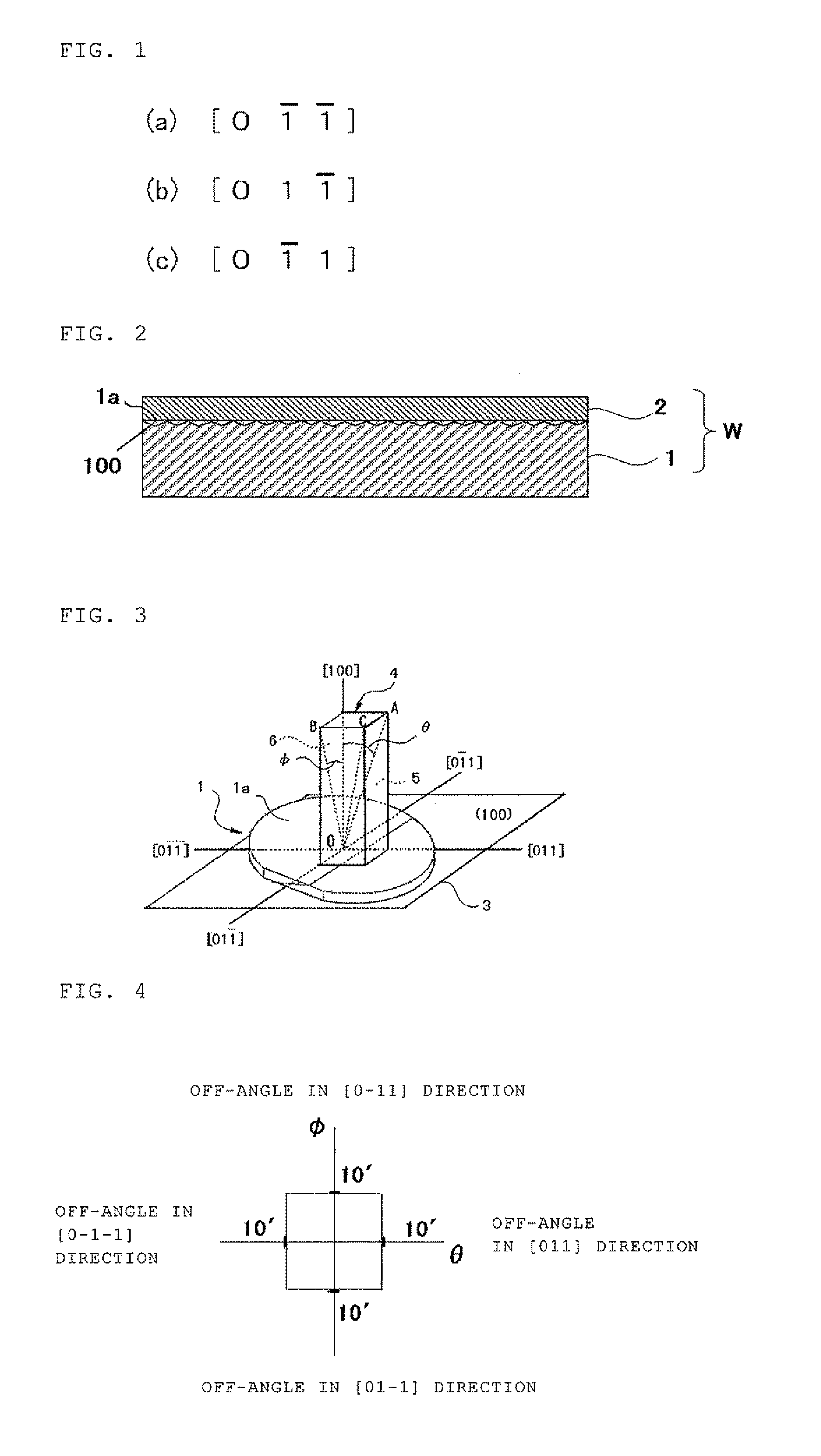
[0082]A 3 μm epitaxial layer was grown on the main surface of each of silicon single crystal substrates (a diameter of 300 mm) by vapor phase epitaxy at a growth temperature of 1080° C. while a phosphine (PH3) gas was introduced in conditions where the concentration of phosphorus in the epitaxial layer became 2×10¹⁹ / cm3. The main surface of each of the silicon single crystal substrates was tilted with respect to the [100] axis at an angle θ in the [011] direction from the (100) plane and at an angle φ in the [01-1] direction from the (100) plane, where the angle θ satisfied 6′ (0.1°)≦θ≦9′ (0.15°) and the angle φ was 1 minute. The material gas used herein was dichlorosilane.
example 2
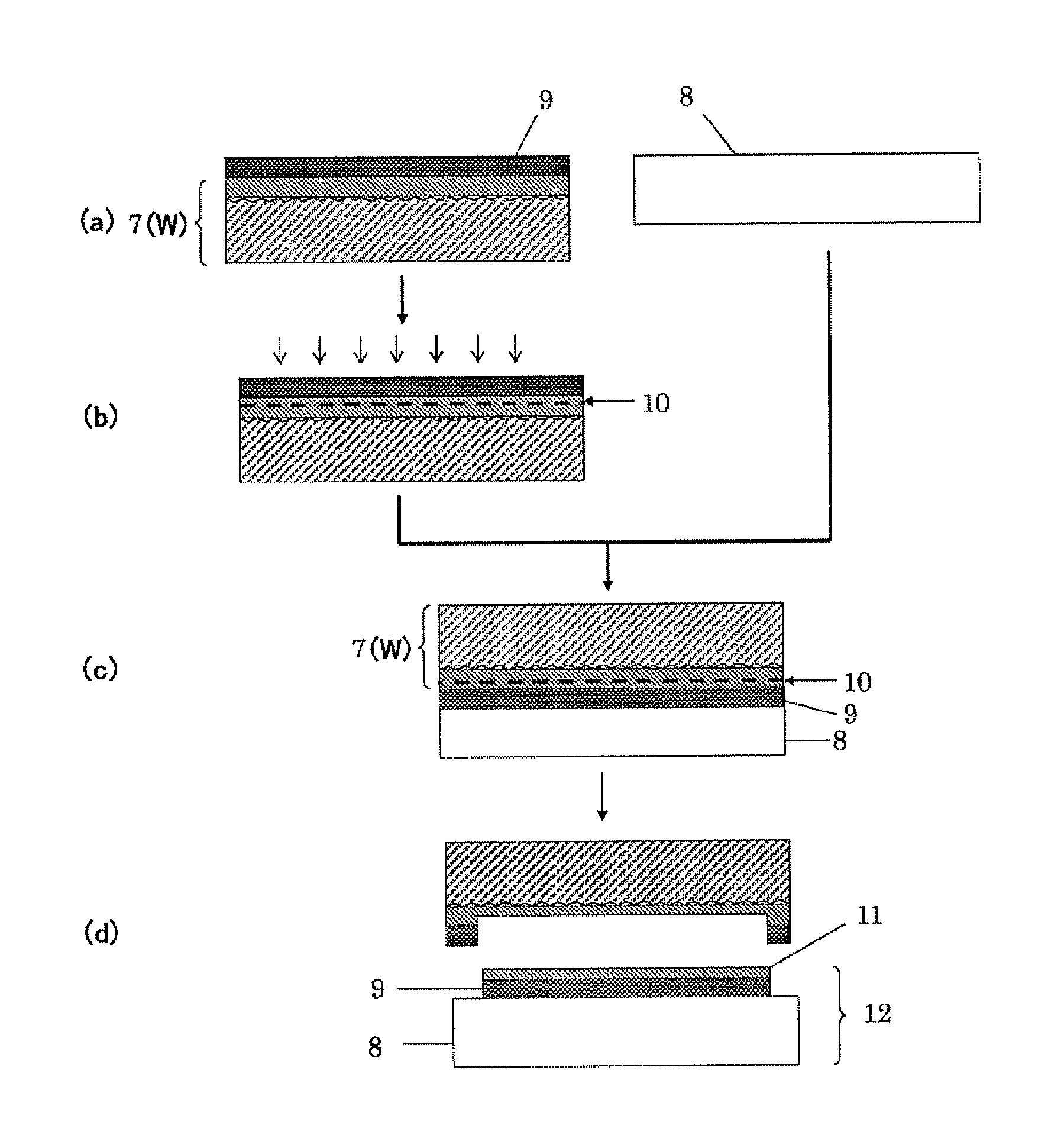
[0091]The epitaxial wafer obtained in Example 1 was used as the bond wafer (the wafer for forming the SOI layer) to manufacture the bonded SOI wafer according to the method for manufacturing a bonded SOI wafer (using the ion implantation delamination method) shown in FIG. 8. The manufacture conditions will be described below.
(BOND WAFER): The epitaxial wafer manufactured in Example 1.
(BASE WAFER): A silicon single crystal substrate; a diameter of 300 mm; p-type, (100); 10 Ωcm.
(FORMATION OF OXIDE FILM): A 150 nm thermal oxide film formed on the surface of the bond wafer.
(ION IMPLANTATION): Hydrogen ions implanted through the oxide film on the surface of the bond wafer; 50 keV; 6×10¹⁶ / cm2.
(DELAMINATION HEAT TREATMENT): 500° C.; 30 minutes.
[0092]The bonding heat treatment was performed on the SOI wafer after delamination under an oxidizing atmosphere. After removing the oxide film from the surface, a flattening heat treatment was performed at 1200° C. under an Ar atmosphere for one hou...
PUM
 Abstract
Description
Claims
Application Information


