Organic semiconductor thin film, organic semiconductor device and organic field effect transistor

a technology of organic semiconductor and semiconductor material, which is applied in the direction of thermoelectric devices, instruments, organic chemistry, etc., can solve the problems of difficult synthesis of organic semiconductor material in which both chemical stability and high carrier mobility are satisfied, and difficult industrial application of material groups, etc., to achieve the effect of superior organic fet characteristics

Inactive Publication Date: 2015-01-06
JNC CORP +1
View PDF15 Cites 2 Cited by
  • Summary
  • Abstract
  • Description
  • Claims
  • Application Information

AI Technical Summary

Benefits of technology

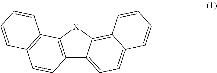
[0040]An organic semiconductor thin film of the invention includes a specific compound that is easily synthesized, and is chemically and physically stable, and has a W-shaped structure, and therefore can be industrially manufactured, and shows a high carrier mobility than can be utilized in an organic semiconductor application by an improvement in molecular interaction utilizing a chalcogen element present in a bent site of the W-shaped structure.

Problems solved by technology

The polyacene compound is generally unstable to light or oxidization, and therefore is a material group that is difficult to be industrially applied.
However, as a molecular structure becomes more complicated, the compounds can be barely synthesized by using an expensive raw material and a reactant having a high environmental load, and through multi-step synthesis.
Thus, a variety of organic semiconductor materials have been developed so far, but synthesis of an organic semiconductor material in which both the chemical stability and the high carrier mobility are satisfied has been difficult through an industrially applicable route.
However, no substantial study has been made on utilization as the organic semiconductor material.
However, any semiconductor characteristics are not specifically disclosed, and any compound other than dinaphthothiophene, any compound having a U-shaped structure and any compound having a W-shaped structure are not disclosed.

Method used


Image

  • Organic semiconductor thin film, organic semiconductor device and organic field effect transistor
  • Organic semiconductor thin film, organic semiconductor device and organic field effect transistor
  • Organic semiconductor thin film, organic semiconductor device and organic field effect transistor

Examples


example 1

Preparation of an Organic Transistor by a Single Crystal Process and Evaluation of Characteristics of the Organic Transistor

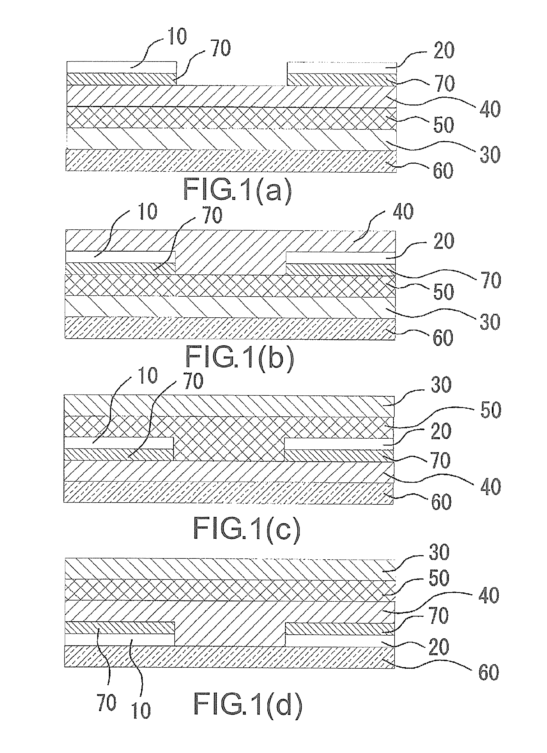
[0076]Ultrasonic cleaning was applied to a silicon substrate with a thermally oxidized silicon insulating film (film thickness: 500 nm) for 5 minutes by using each of acetone and 2-propanol, and subsequently UV ozone treatment was applied to the substrate for 30 minutes. On a surface of the substrate subjected to cleaning treatment, a self-assembled monolayer (SAM) of triethoxytridecafluorooctylsilane (FDTS) was formed according to a vapor process.

[0077]Independently thereof, a single crystal film of an organic semiconductor material as shown in Table 1 was prepared according to a physical vapor transport process for allowing crystals to gradually grow by means of a tube furnace having a temperature gradient, and the resultant single crystal film was placed on a substrate. In addition, the physical vapor transport process was applied under the conditions of a t...

example 2

Preparation of an Organic Transistor by a Single Crystal Process and Evaluation of Characteristics of the Organic Transistor

[0079]A bottom gate-top contact type organic FET (channel length: 500 μm, channel width: 1 mm) was prepared in a manner similar to Example 1 except that an organic semiconductor material in Table 1 was used, and a carrier mobility and an ON-OFF ratio were measured. The results are shown in Table 1.

example 3

Preparation of an Organic Transistor by a Single Crystal Process and Evaluation of Characteristics of the Organic Transistor

[0080]A bottom gate-top contact type organic FET (channel length: 1,000 μm, channel width: 1 mm) was prepared in a manner similar to Example 1 except that an organic semiconductor material in Table 1 was used, and a self-assembled monolayer (SAM) was not formed, and a carrier mobility and an ON-OFF ratio were measured. The results are shown in Table 1.


PUM

PropertyMeasurementUnit
carrier mobilityaaaaaaaaaa
thicknessaaaaaaaaaa

Abstract

An organic semiconductor thin film including an organic semiconductor material that is easily synthesized, and is chemically and physically stable, and shows a high carrier mobility, an organic semiconductor device and an organic field effect transistor including the organic semiconductor thin film are provided. An organic semiconductor thin film of the invention includes a compound represented by the following formula 1:wherein, in formula (1), X is oxygen, sulfur or selenium.

Description

CROSS REFERENCE TO RELATED APPLICATIONS[0001]This application claims the priority benefit of Japan application serial no. 2012-060908, filed on Mar. 16, 2012. The entirety of the above-mentioned patent application is hereby incorporated by reference herein and made a part of this specification.BACKGROUND OF THE INVENTION[0002]1. Field of the Invention[0003]The present invention relates to an organic semiconductor thin film, and an organic semiconductor device and an organic field effect transistor both including the organic semiconductor thin film.[0004]2. Related Art[0005]In recent years, an organic compound having semiconductor characteristics has attracted attention. Among the organic compounds, a polyacene compound such as pentacene and tetracene has been known as an organic semiconductor material due to a high carrier mobility thereof for many years. In addition, “carrier mobility” herein is used in a broad sense, including an electron mobility and a hole mobility.[0006]The pol...

Claims


Application Information

Patent Timeline
Patent Type & Authority Patents(United States)
IPC IPC(8): H01L35/24C07D333/50H01L51/05H01L51/00
CPCH01L51/0074H01L51/0071H01L51/0073H01L51/0541H01L51/0545C09B57/00H10K85/657H10K85/6574H10K85/6576H10K10/464H10K10/466H10K10/484
Inventor TAKEYA, JUNICHIOKAMOTO, TOSHIHIRONAKANISHI, TAUTO
Owner JNC CORP
Why Eureka
Try Eureka