
Large diamond crystal substrates and methods for producing the same

a diamond crystal and substrate technology, applied in the field of can solve the problems of not being able to produce single crystal diamond substrates with a larger area, not being able to easily increase the substrate area of these substrates, and not being able to achieve the effect of large surface area, convenient treatment or processing, and uniform properties

Active Publication Date: 2015-01-27
NAT INST OF ADVANCED IND SCI & TECH
View PDF20 Cites 10 Cited by
  • Summary
  • Abstract
  • Description
  • Claims
  • Application Information

AI Technical Summary

Benefits of technology

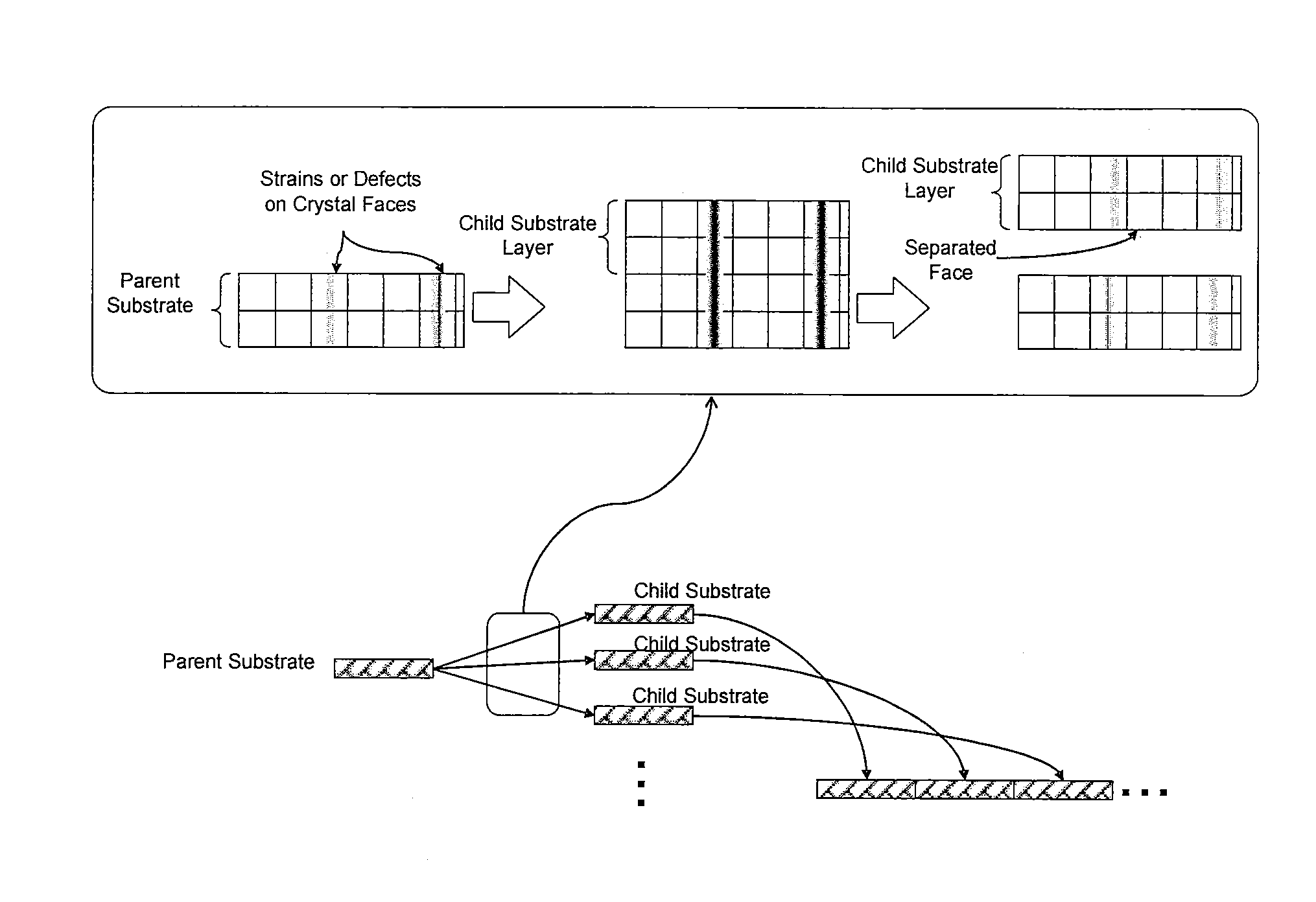
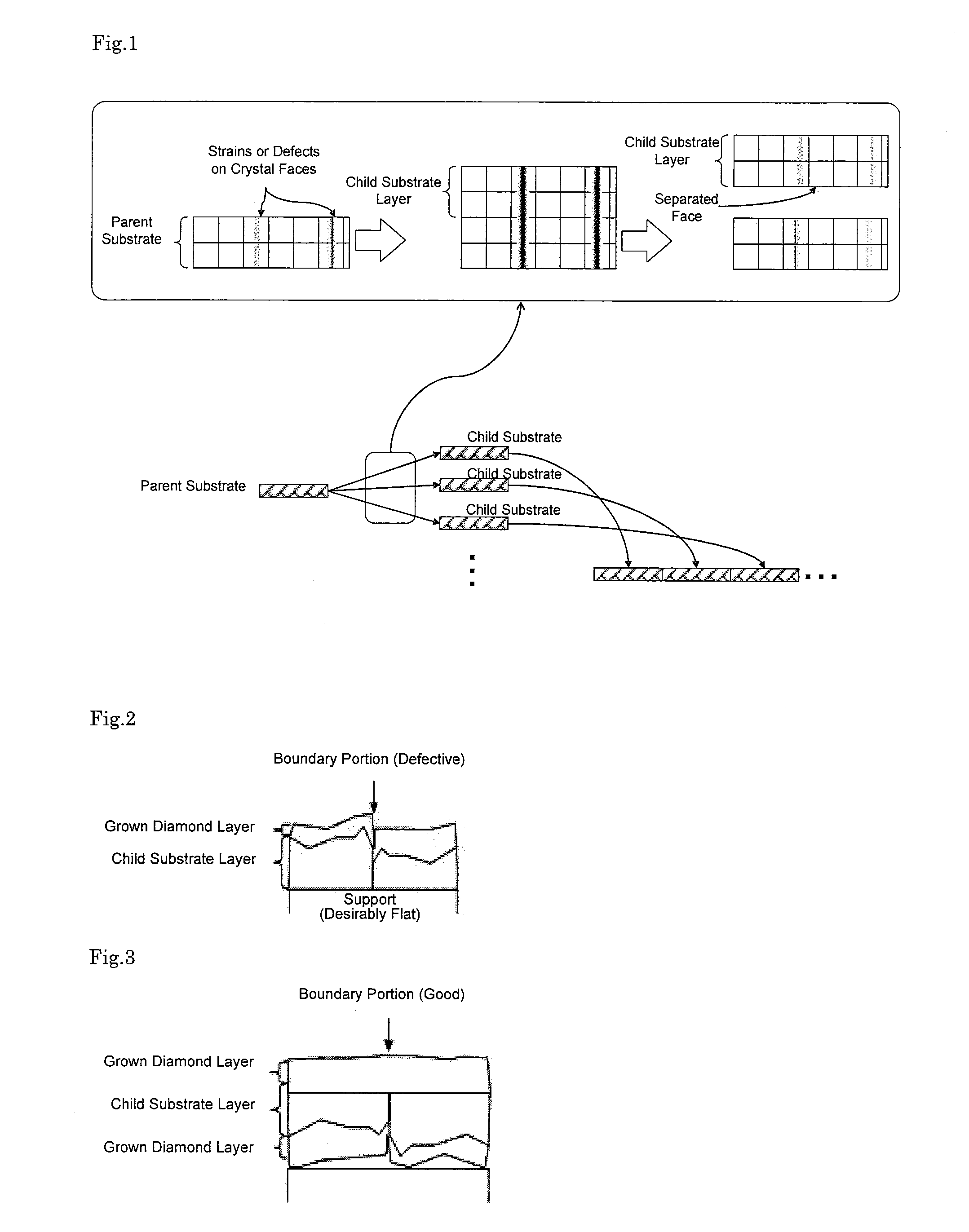
This patent describes a method for producing a large single-crystal diamond substrate that has uniform properties, such as thickness, off-angle, crystal plane direction, strain distribution, and defect distribution. This allows for the growth of uniform diamond layers without needing to vary the diamond growth conditions for each child substrate. The method also enables easy preparation of a large mosaic substrate of single-crystal diamond, which is particularly suitable for practical use as a semiconductor material. The invention can be applied to a variety of wide bandgap semiconductor single crystals, such as SiC, GaN, AlN, and ZnO.

Problems solved by technology

Of these methods, the high-pressure synthesis method can produce substrates with an area of only up to about 1×1 cm, and cannot be expected to produce single-crystal substrates with a larger area.
Furthermore, single-crystal diamond substrates with an area of about 5×5 mm or more are not readily available, nor is it easy to increase the substrate area of these substrates.
However, during epitaxial growth of diamond by a vapor-phase synthesis method, many defects such as non-epitaxial crystallites and hillocks tend to occur, making the synthesis of a large single-crystal diamond difficult.
Thus, the properties of the growth layers do not become uniform, unless the synthesis conditions are adjusted according to the off-angle and off-direction of each substrate during the growth of single-crystal diamond on substrates having different off-angles and off-directions.
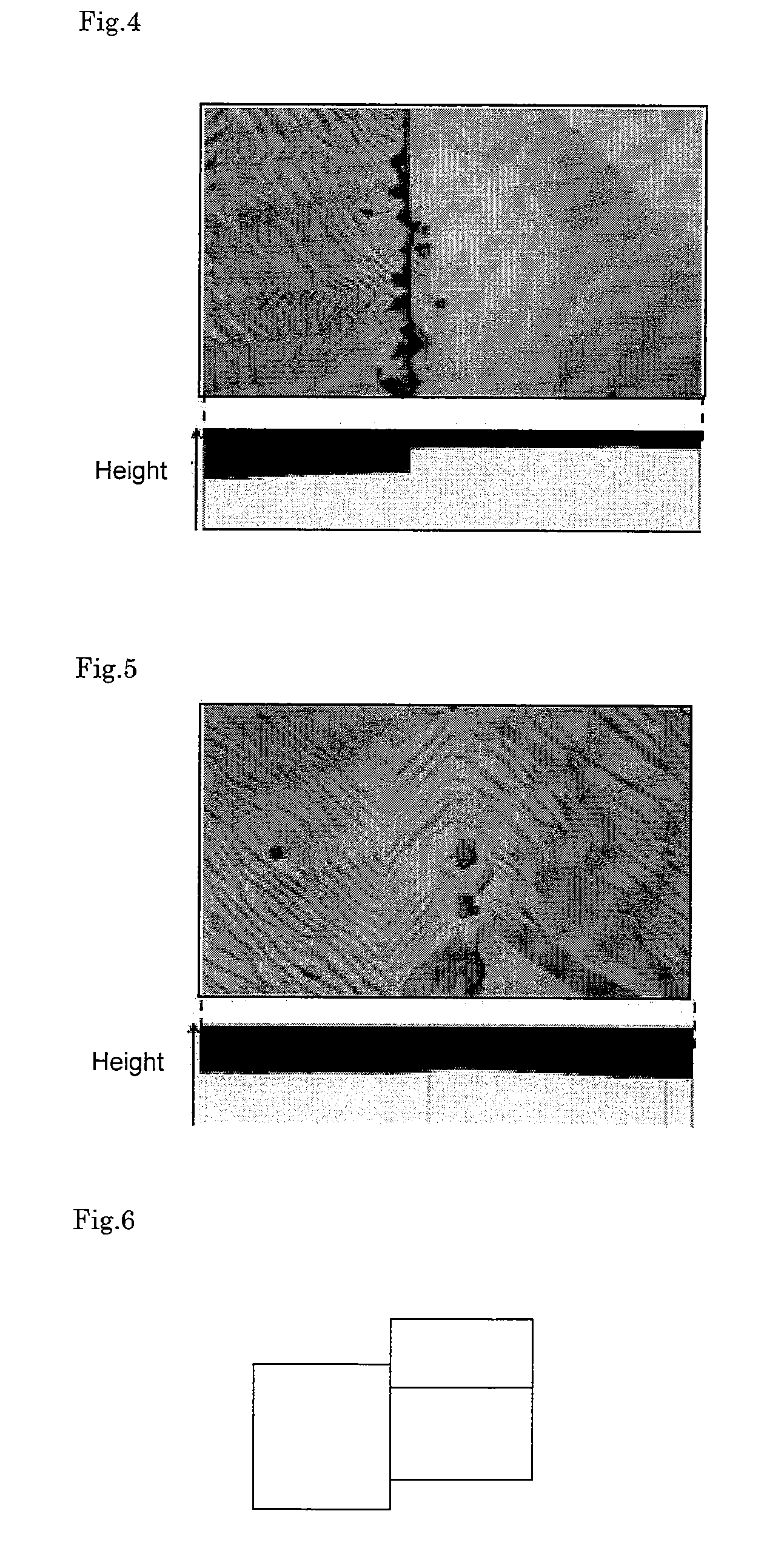
Defects on the substrate surface are also continued in the growth layer, and the positions of these defects cannot be controlled for each substrate.
Therefore, the presence of these defects is one hindrance to achieving uniform growth layer properties.
Similar problems also arise in the method described above, wherein substrates with different off-angles and off-directions are positively used and bonded with one another to produce a mosaic substrate (see Japanese Unexamined Patent Publication No. 2006-306701).
Nevertheless, none of the previously known methods for producing mosaic substrates have proposed an effective solution to make the properties of substrates to be bonded uniform.
Therefore, if large diamond wafers obtained using any of the above-mentioned methods do not have a uniform off-angle, off-direction, strain distribution, defect distribution, etc., it is expected that the devices prepared thereon will also exhibit non-uniform properties.
Therefore, the use of these mosaic wafers with non-uniform properties will obviously result in an extremely low yield of devices that can withstand practical use.
Further, because mosaic diamond substrates must be strong enough to withstand processing for device preparation, it is sometimes necessary to additionally grow a single-crystal diamond onto the bonded substrates.
If the single-crystal diamonds used as the substrates to be bonded have different properties, it will be difficult to uniformly grow the single-crystal diamond on the bonded substrates.
Furthermore, as mentioned above, it is difficult to obtain a desired number of crystals whose substrate properties are uniform.
For example, the preparation of diamond substrates that meet predetermined requirements by processing a single-crystal diamond requires a great deal of time, because processing of the diamond crystal is very difficult; moreover, the preparation of a precisely processed single-crystal diamond substrate is difficult.
In particular, it is impossible to impart specific strain and defect distributions to a given substrate.
For reasons as stated above, despite their high demand, single-crystal diamond substrates with a large area that can withstand practical use are not available yet.

Method used


Image

  • Large diamond crystal substrates and methods for producing the same
  • Large diamond crystal substrates and methods for producing the same
  • Large diamond crystal substrates and methods for producing the same

Examples


example 1

[0142]A single-crystal diamond (100) substrate having dimensions of 3×3×0.5 mm3 was used as a parent substrate, and a large single-crystal diamond substrate was prepared according to the following method.

[0143]Carbon ions were first implanted into the single-crystal diamond substrate at an implantation energy of 3 MeV and a dose of 2×10¹⁶ ions / cm2, using a 1.5 MV tandem accelerator. The calculated value of the ion implantation depth was about 1.6 μm. After the radiation, the diamond substrate changed from transparent to black, which confirmed that a non-diamond layer was formed.

[0144]The single-crystal diamond substrate was subsequently heat-treated using a commercially available microwave plasma CVD apparatus, thereby causing the graphitization of the non-diamond layer to proceed. The conditions for heat treatment were as follows: a substrate temperature of 1,060° C.; a pressure of 16 kPa; a hydrogen gas flow rate of 500 sccm; and a treatment time of 5 minutes. Subsequent to the he...

example 2

[0150]A single-crystal diamond (100) substrate having a diameter of 9 mm and a thickness of 1 mm, and provided with a linear notch was used as a parent substrate, and a large single-crystal diamond substrate was prepared according to the following method.

[0151]The single-crystal diamond substrate was first implanted with ions by the same method as in Example 1. The single-crystal diamond substrate was subsequently heat-treated by the same method as in Example 1, using a commercially available microwave plasma CVD apparatus, thereby causing the graphitization of the non-diamond layer to proceed. The growth of a single-crystal diamond film was subsequently conducted for 3 hours, at a substrate temperature of 1,100° C., a pressure of 15 kPa, a hydrogen gas flow rate of 500 sccm, a methane gas flow rate of 25 sccm, and a nitrogen gas flow rate of 2 sccm.

[0152]The CVD-deposited single-crystal diamond film was then removed from the single-crystal diamond substrate according to the same me...


PUM

PropertyMeasurementUnit
off-anglesaaaaaaaaaa
off-angleaaaaaaaaaa
off-angleaaaaaaaaaa

Abstract

The present invention provides a method for producing a large substrate of single-crystal diamond, including the steps of preparing a plurality of single-crystal diamond layers separated form an identical parent substrate, placing the single-crystal diamond layers in a mosaic pattern on a flat support, and growing a single-crystal diamond by a vapor-phase synthesis method on faces of the single-crystal diamond layers where they have been separated from the parent substrate.According to the method of the invention, a mosaic single-crystal diamond having a large area and good quality can be produced relatively easily.

Description

BACKGROUND OF THE INVENTION[0001](1) Field of the Invention[0002]The present invention relates to single-crystal diamond substrates having a large area, and methods for producing such substrates.[0003](2) Description of the Related Art[0004]Diamond, which exhibits outstanding properties as a semiconductor, is a promising material for use in semiconductor devices, such as high-output power devices, high-frequency devices, light-receiving devices, etc. In particular, in order to realize the practical use of diamond as a semiconductor material, wafers of single-crystal diamond having a large area and uniform quality are required.[0005]Typical methods for growing single-crystal diamond heretofore used include a high-pressure synthesis method and a vapor-phase synthesis method. Of these methods, the high-pressure synthesis method can produce substrates with an area of only up to about 1×1 cm, and cannot be expected to produce single-crystal substrates with a larger area. Furthermore, sin...

Claims


Application Information

Patent Timeline
Patent Type & Authority Patents(United States)
IPC IPC(8): B01J3/06C30B33/06C30B23/00B01J19/08C23C14/00C01B31/06C30B25/00C30B29/04C30B33/00
CPCC30B29/04C30B33/00C30B23/00C01B31/06C01B31/065C30B25/00C30B33/06C01B32/28
Inventor YAMADA, HIDEAKICHAYAHARA, AKIYOSHIMOKUNO, YOSHIAKISHIKATA, SHINICHI
Owner NAT INST OF ADVANCED IND SCI & TECH
Learn More