Copper foil for printed wiring board, method for producing said copper foil, resin substrate for printed wiring board and printed wiring board

a technology of printed wiring and resin substrate, which is applied in the direction of magnetic recording, metal pattern materials, record information storage, etc., can solve the problems of increasing the number of steps, not being suitable for a stable circuitry design, and not being able to detect the impedance, etc., and achieves the effect of higher frequency

Active Publication Date: 2015-05-12
JX NIPPON MINING & METALS CORP
View PDF40 Cites 4 Cited by
  • Summary
  • Abstract
  • Description
  • Claims
  • Application Information

AI Technical Summary

Benefits of technology

[0029]The present invention has advantageous effects. Namely, the copper foil can provide a printed wiring board wherein the adhesiveness with a resin can be enhanced, and peel strength against chemical treatment at the time of forming a fine pattern on a package board can be increased to allow fine etching. The copper foil is also useful for a method of increasing adhesion strength with a copper layer for a circuit (e.g. a non-electrolytic plating layer) subsequently formed on a surface of a resin by once removing a copper layer completely to transfer a roughened surface to the resin.
[0030]In the context of an increasingly finer pattern and increasingly higher frequency for a printed circuit in recent years, it is particularly effective for a semiconductor package board produced by combining a copper foil for a printed circuit (a copper foil for a semiconductor package board) and a copper foil for a semiconductor package board with a resin for a semiconductor package.

Problems solved by technology

When a frequency of an electric signal is 1 GHz or higher, the skin effect, in which an electric current flows only on the surface of a conductor, becomes significant, and an uneven surface causes a change in electric current transmission paths, resulting in a non-negligible increase in impedance.
Although this has an effect of preventing “powder fall,” a problem is that the number of steps is increased, and that the effects of preventing “powder fall” vary because the copper plating is thin.
Therefore, there exists a problem that it is unsuitable for a stable circuitry design.
However, when a printed circuit board over which a heat resistant layer of brass is formed was subject to etching treatment with a hydrochloric acid based etching solution (for example, CuCl2, FeCl3), and an unwanted region of the copper foil except for a region of the printing circuit was removed to form a conductive circuit, a phenomenon of so-called erosion (circuit erosion) occurred at the both ends of the circuit pattern, causing a problem that the peel strength with the resin substrate was deteriorated.
The phenomenon of circuit erosion is referred to as a phenomenon where erosion occurs by the aforementioned etching solution at the adhesion interface layer between a copper foil of a circuit formed by the aforementioned etching treatment and a resin substrate, i.e. at the side of etching where the heat resistant and rust proof layer of brass is exposed, and the both ends, which are otherwise normally yellow (because it is made of brass), become red due to the erosion because water washing is insufficient, resulting in significantly deteriorated peel strength in those regions.
Thus, if this phenomenon occurs over an entire circuit pattern, the circuit pattern will be detached from the substrate, causing a problem.

Method used


Image

  • Copper foil for printed wiring board, method for producing said copper foil, resin substrate for printed wiring board and printed wiring board
  • Copper foil for printed wiring board, method for producing said copper foil, resin substrate for printed wiring board and printed wiring board

Examples


example 1

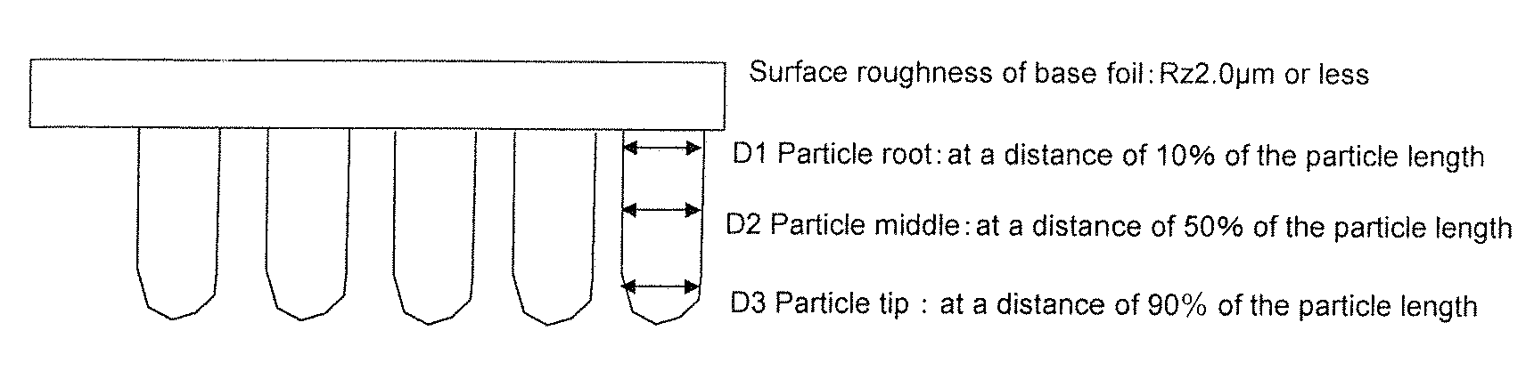
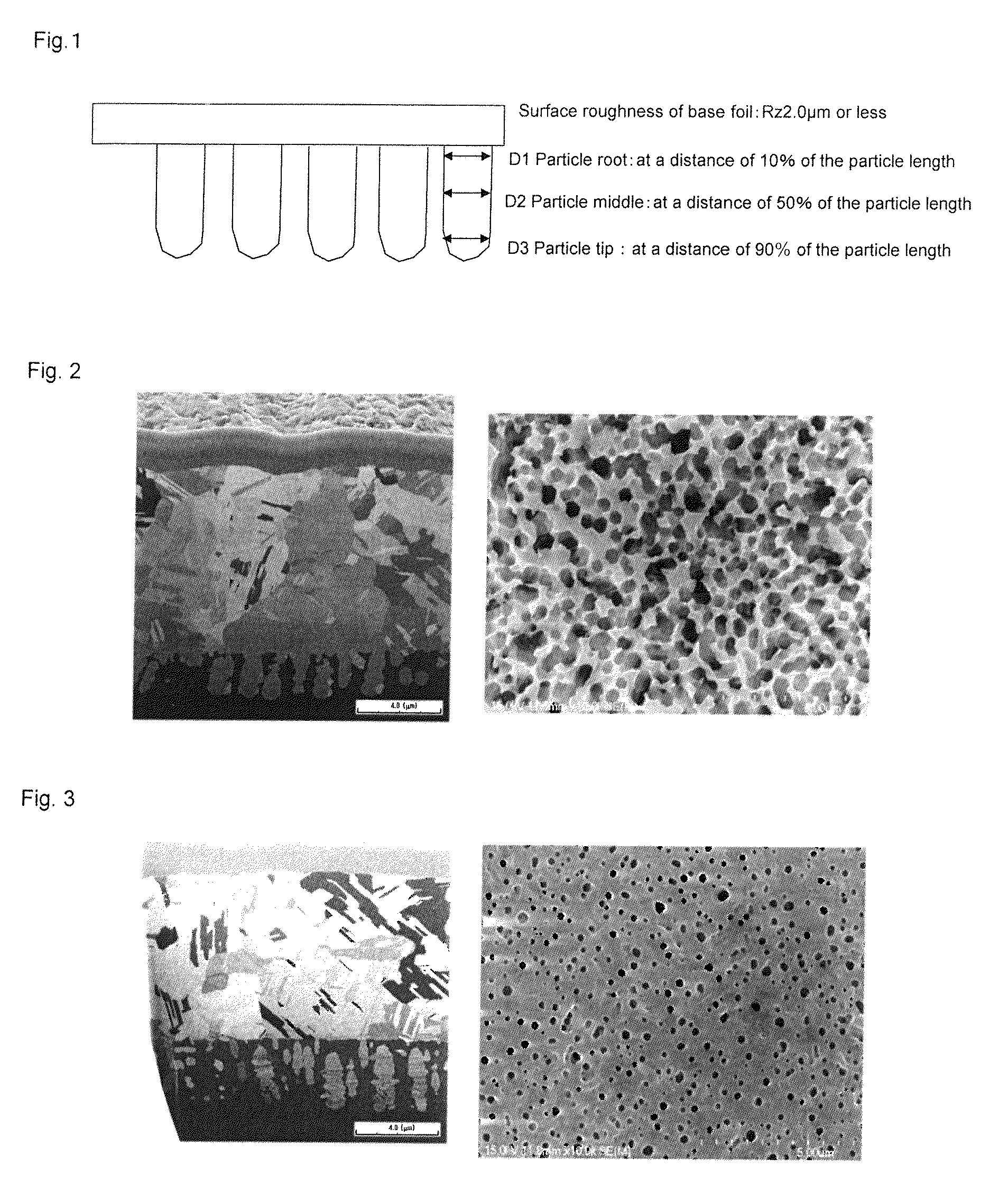
[0091]Using a 12 μm-thick electrolytic copper foil (the roughness of a surface on which a roughened copper layer is formed: Rz 0.6 μm), roughening plating was performed on the rough surface (namely ‘matte surface’ or ‘M surface’) of this copper foil as described below. The treatment conditions are shown below. Each of these is a step for forming a roughened layer on the copper foil of the present invention. The ratio to the limiting current density when forming roughening particles was 2.50.

(Liquid Composition 1)

[0092]CuSO4.5H2O: 58.9 g / L

[0093]Cu: 15 g / L

[0094]H2SO4: 100 g / L

[0095]Na2WO4.2H2O: 5.4 mg / L

[0096]W: 3 mg / L

[0097]Added amount of sodium dodecyl sulfate: 10 ppm

[0098](Electroplating Temperature 1) 50° C.

[0099]Normal plating as shown below was performed after the present roughening treatment. The treatment conditions are shown below.

(Liquid Composition 2)

[0100]CuSO4′5H2O: 156 g / L

[0101]Cu: 40 g / L

[0102]H2SO4: 100 g / L

[0103](Electroplating Temperature 1) 40° C.

(Electric Current Condi...

example 2

[0124]Using a 12-μm thick electrolytic copper foil, roughening plating as described below and normal plating as in Example 1 were performed on a rough surface (a matte surface) of that copper foil. The treatment conditions for roughening plating are shown below. Each of these is a step for forming a roughened layer on the copper foil of the present invention. The ratio to the limiting current density when forming roughening particles was 3.10.

(Liquid Composition 1)

[0125]CuSO4.5H2O: 58.9 g / L

[0126]Cu: 15 g / L

[0127]H2SO4: 100 g / L

[0128]Na2WO4.2H2O: 5.4 mg / L

[0129]W: 3 mg / L

[0130]Added amount of sodium dodecyl sulfate: 10 ppm

[0131](Electroplating Temperature 1) 50° C.

[0132]The surface roughness Rz of this roughened layer is 1.51 μm, and the average diameter at the particle root (D1) is 0.51 μm, and the particle length (L1) is 2.68 μm, and the ratio to the average diameter at the particle root (D1) is 5.21 when L1 / D1. Needle-like or rod-like particles appear to be formed by the look of FIG. ...

example 3

[0138]Using a 12-μm thick electrolytic copper foil, roughening plating as described below and normal plating as in Example 1 were performed on a rough surface (a matte surface) of that copper foil. The treatment conditions for roughening plating are shown below. Each of these is a step for forming a roughened layer on the copper foil of the present invention. The ratio to the limiting current density when forming roughening particles was 4.30.

(Liquid Composition 1)

[0139]CuSO4.5H2O: 58.9 g / L

[0140]Cu: 15 g / L

[0141]H2SO4: 100 g / L

[0142]Na2WO4.2H2O: 5.4 mg / L

[0143]W: 3 mg / L

[0144]Added amount of sodium dodecyl sulfate: 10 ppm

[0145](Electroplating Temperature 1) 50° C.

[0146]The surface roughness Rz of this roughened layer is 1.56 μm, and the average diameter at the particle root (D1) corresponding to a distance of 10% of a particle length is 0.59 μm. The particle length (L1) is 2.68 μm, and the ratio to the average diameter at the particle root (D1) is 4.52 when L1 / D1. By the look of FIG. 2,...


PUM

PropertyMeasurementUnit
lengthaaaaaaaaaa
diameteraaaaaaaaaa
widthaaaaaaaaaa

Abstract

A copper foil for a printed wiring board, the copper foil being characterized by having, on at least one surface thereof, a roughed layer of the copper foil in which an average diameter at a particle root (D1) corresponding to a distance of 10% of a particle length from the root, is 0.2 μm to 1.0 μm, and a ratio of the particle length (L1) to the average diameter at the particle root (D1) is 15 or less when L1 / D1. A copper foil for a printed wiring board, wherein a sum of area covered by holes on an uneven and roughened surface of a resin is 20% or more at a surface of the resin formed by laminating the resin and a copper foil for a printed wiring having a roughened layer and then removing the copper layer by etching. An object of the present invention is to develop a copper foil for a semiconductor package board in which the aforementioned phenomenon of circuit erosion is avoided without deteriorating other properties of the copper foil. In particular, an object of the present invention is to provide a copper foil for a printed wiring board and a producing method thereof, wherein a roughened layer of the copper foil can be improved to enhance the adhesiveness between the copper foil and a resin.

Description

BACKGROUND[0001]The present invention relates to a copper foil for a printed wiring board having excellent chemical resistance and adhesiveness, a producing method thereof, a resin substrate for a printed wiring board and a printed wiring board. In particular, the present invention provides a copper foil and a producing method thereof as well as a printed wiring board, wherein strong peel strength against chemical treatment when forming a fine pattern on a package board such as a BT (bismaleimide triazine) resin impregnated substrate can be obtained to allow fine etching. Further, the present invention provides a copper foil for a printed wiring board, a producing method thereof, a resin substrate for a printed wiring board and a printed wiring board, wherein peel strength can be improved significantly in a method of forming a copper pattern by non-electrolytic plating after complete etching of a surface of the copper foil.[0002]A copper foil for a semiconductor package board, which...

Claims


Application Information

Patent Timeline
Patent Type & Authority Patents(United States)
IPC IPC(8): H05K3/38C25D5/10C25D1/04H05K3/02C25D5/12C23C18/16B32B15/20H05K1/09C25D11/38H05K3/06C25D3/38C25D5/16C25D7/06
CPCH05K3/06C25D11/38C25D5/12Y10T428/24355C25D5/10Y10T428/12431Y10S428/935Y10T428/12549C23C18/1651C25D3/38C25D5/16H05K3/022H05K3/38C25D7/0614H05K1/09C25D1/04C23C28/023H05K3/383H05K2201/0355C25D5/605H05K3/384H05K3/388H05K2201/0358H05K2203/0307Y10T428/12063Y10T428/12438Y10T428/12472Y10T428/1291Y10T428/12993C25D7/06
Inventor KOHIKI, MICHIYAMORIYAMA, TERUMASA
Owner JX NIPPON MINING & METALS CORP
Why Eureka
Try Eureka