Liquid crystal polymer copper-clad laminate and copper foil used for said laminate

a technology of liquid crystal polymer and copper foil, which is applied in the direction of circuit optical details, transportation and packaging, and the improvement of the adhesion of metals to the insulation substrate, etc., can solve the problems of generating roughening particle residues, and achieve excellent peeling strength, improved etching properties, and high accuracy

Active Publication Date: 2015-06-16
JX NIPPON MINING & METALS CORP
View PDF40 Cites 7 Cited by
  • Summary
  • Abstract
  • Description
  • Claims
  • Application Information

AI Technical Summary

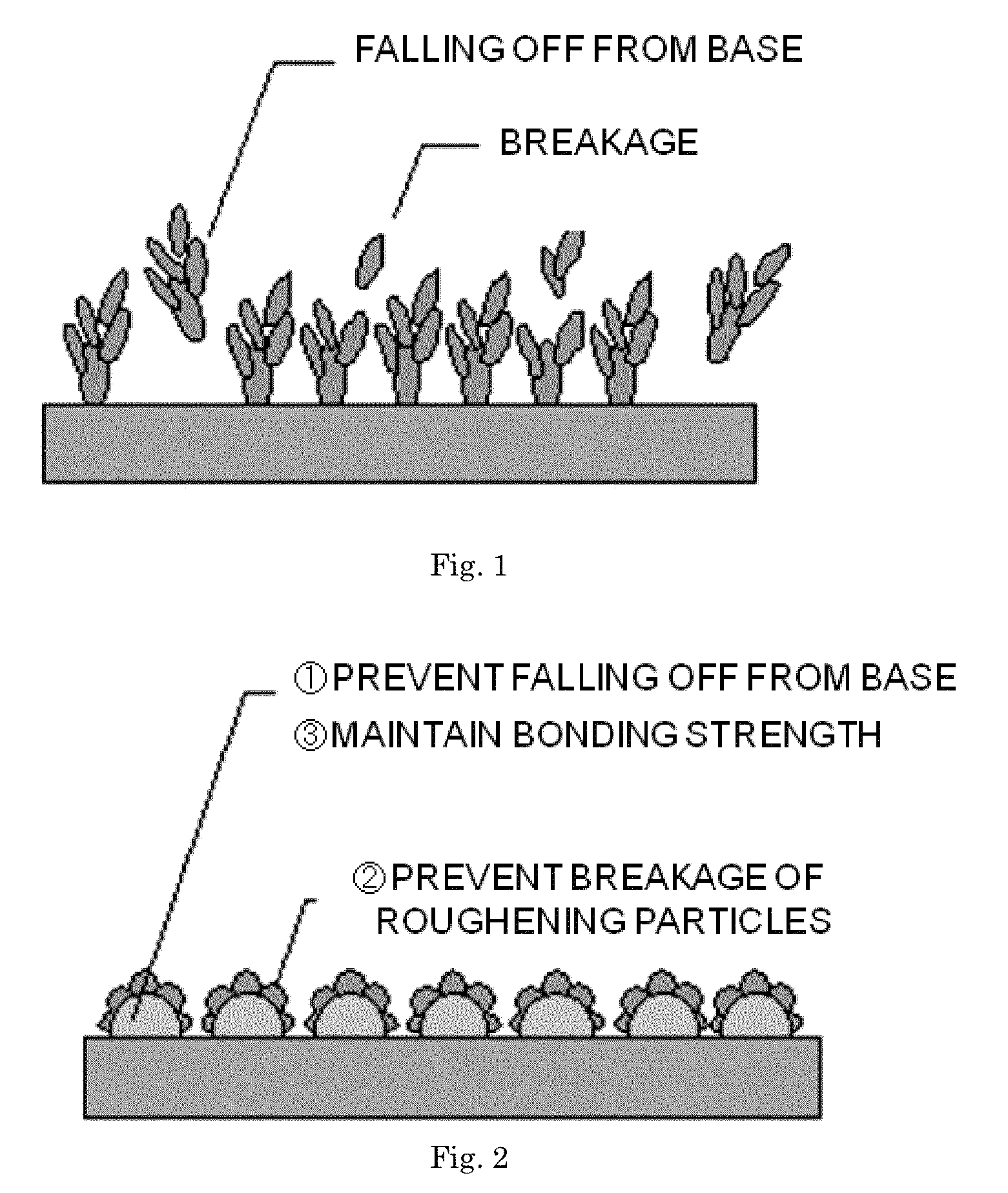
Benefits of technology

[0031]A copper-clad laminate according to the present invention has excellent peel strength with a liquid crystal polymer (LCP) and has a property of not generating a roughening particle residue on a surface of the liquid crystal polymer after circuit etching.
[0032]Also, since abnormally grown particles are reduced, particle size becomes uniform, and it is possible to cover an entire surface, etching property is improved, making it possible to form a circuit with high accuracy.
[0033]Along with the development of electronic appliances, downsizing and high integration of semiconductor devices have further progressed. There is a severer demand for the treatments performed in production processes of printed circuits for the semiconductor devices. The present invention has the technological effects which meet the demand.

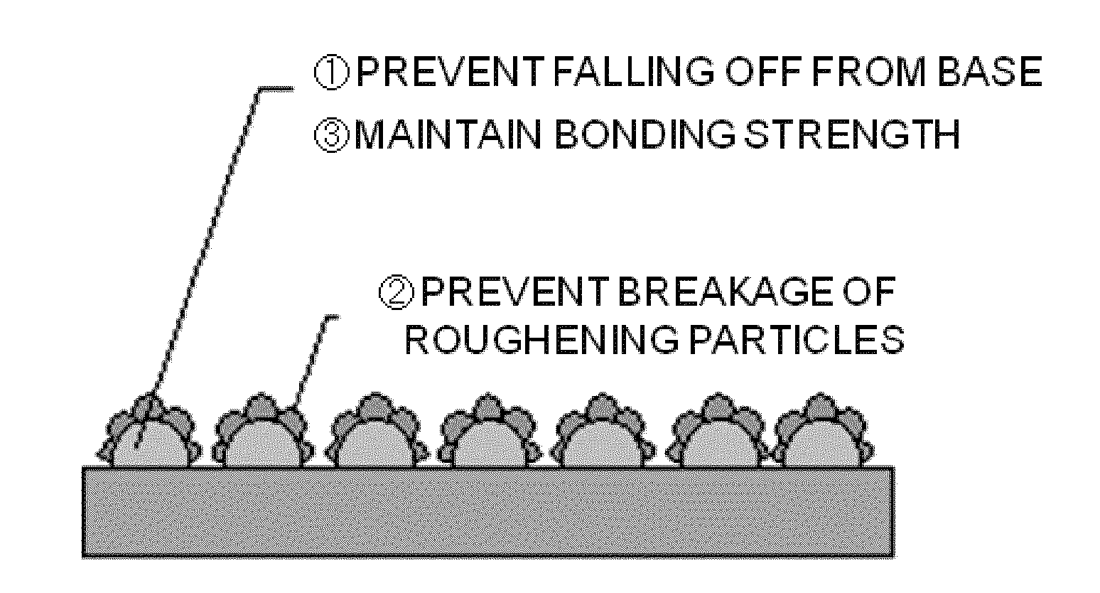
Problems solved by technology

However, in the printed circuit board using the liquid crystal polymer, in the case of using the copper foil for printed circuit referred to in Patent Literature 2, which is obtained by performing roughening treatment with copper-cobalt-nickel alloy plating on a surface of the copper foil, forming a cobalt-nickel alloy-plated layer, and then forming the zinc-nickel alloy-plated layer, there arises a problem of roughening particle residue which is generated on the liquid crystal polymer resin surface after the circuit etching in the fine pattern circuit of the copper-clad laminate is detected.

Method used


Image

  • Liquid crystal polymer copper-clad laminate and copper foil used for said laminate
  • Liquid crystal polymer copper-clad laminate and copper foil used for said laminate
  • Liquid crystal polymer copper-clad laminate and copper foil used for said laminate

Examples


example 1 to example 9

[0112]A primary particle layer (Cu) and a secondary particle layer (copper-cobalt-nickel alloy plating) were formed on a rolled copper foil having a thickness of 12 μm under the below-described conditions.

Bath compositions and plating conditions are as follows.

Bath Composition and Plating Conditions

[0113](A) Formation of Primary Particle Layer (Cu Plating)

[0114]Liquid composition: 15 μg / L of copper, 75 μg / L of sulfuric acid

[0115]Liquid temperature: 35° C.

[0116]Current density: 48 to 60 A / dm2 and 1 to 10 A / dm2

[0117]Coulomb amount: 70 to 90 As / dm2 and 5 to 20 As / dm2

[0118](B) Formation of Secondary Particle Layer (Cu—Co—Ni Alloy Plating)

[0119]Liquid composition: 15 g / L of copper, 8 g / L of nickel, 8 g / L of cobalt

[0120]pH: 2

[0121]Liquid temperature: 40° C.

[0122]Current density: 10 to 33 A / dm2

[0123]Coulomb amount: 30 to 45 As / dm2


PUM

PropertyMeasurementUnit
particle sizeaaaaaaaaaa
roughness Rzaaaaaaaaaa

Abstract

Provided is a copper-clad laminate obtainable by bonding a copper foil on which roughening treatment including copper-cobalt-nickel alloy plating is performed and a liquid crystal polymer to each other, wherein the copper-clad laminate is free from a roughening particle residue on a surface of the liquid crystal polymer resin after copper foil circuit etching. The copper-clad laminate obtainable by bonding a copper foil and a liquid crystal polymer to each other, wherein the copper foil includes a copper primary particle layer formed on a surface bonded to the liquid crystal polymer and a secondary particle layer formed on the primary particle layer and made from a ternary alloy including copper, cobalt, and nickel; the primary particle layer has an average particle size of 0.25 to 0.45 μm; and the secondary particle layer has an average particle size of 0.05 to 0.25 μm.

Description

TECHNICAL FIELD[0001]The present invention relates to a liquid crystal polymer copper-clad laminate and, particularly, to a liquid crystal polymer copper-clad laminate used for a high frequency printed circuit board. Also, the invention relates to a copper foil used for the liquid crystal polymer copper-clad laminate.[0002]Copper and copper alloy foils (hereinafter collectively referred to as copper foil) greatly contributes to the development of electric and electronic-related industries and, particularly, serve as an indispensable material as a printed circuit material. In general, a copper foil for printed circuit board is laminate-bonded to a substrate such as a synthetic resin board and a film under high temperature and pressure with or without an adhesive agent to produce a copper-clad laminate. After that, in order to form a desired circuit, a resist coating step and an exposure step are performed to print a necessary circuit, and then etching for eliminating unnecessary port...

Claims


Application Information

Patent Timeline
Patent Type & Authority Patents(United States)
IPC IPC(8): B32B5/20H05K3/38C25D7/06H05K1/02C25D5/10C25D5/48H05K1/09C25D3/38C25D3/58C25D5/12C25D11/38
CPCH05K1/0274C25D7/0614H05K3/384C25D5/10C25D5/48Y10T428/12049H05K1/09H05K2201/0141H05K2201/0355C25D3/38C25D3/58C25D5/12C25D11/38C25D5/605B32B15/08
Inventor ARAI, HIDETAKAMINAGA, KENGOMIKI, ATSUSHIFUKUCHI, RYO
Owner JX NIPPON MINING & METALS CORP
Why Eureka
Try Eureka