Epitaxial wafer for heterojunction type field effect transistor

a field effect transistor and epitaxial wafer technology, applied in the direction of basic electric elements, electrical equipment, semiconductor devices, etc., can solve the problem of high cost of the gan substrate, and achieve the effect of reducing the warpage of the nitride-based semiconductor epitaxial wafer and reducing the edge dislocation density

Active Publication Date: 2015-08-18
MURATA MFG CO LTD
View PDF8 Cites 3 Cited by
  • Summary
  • Abstract
  • Description
  • Claims
  • Application Information

AI Technical Summary

Benefits of technology

[0015]By using the above-described combination of the stepwisely composition-graded buffer layer structure and the superlattice buffer layer structure in the present invention, the warpage of the nitride-based semiconductor epitaxial wafer can be reduced significantly and the nitride-based semiconductor epitaxial wafer having a reduced edge dislocation density can be also obtained.

Problems solved by technology

In formation of a heterojunction structure formed of nitride-based semiconductors such as AlGaN layer / GaN layer, these layers have been conventionally formed through epitaxial crystal growth onto a sapphire substrate or a Si substrate because a GaN substrate is expensive.

Method used


Image

  • Epitaxial wafer for heterojunction type field effect transistor
  • Epitaxial wafer for heterojunction type field effect transistor
  • Epitaxial wafer for heterojunction type field effect transistor

Examples


example 1

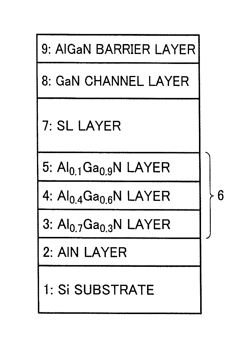
[0021]FIG. 1 is a schematic cross sectional view showing a lamination structure in an epitaxial wafer for a heterojunction type FET according to an example 1 of the present invention.

[0022]For fabrication of this wafer in FIG. 1, a Si substrate 1 having a diameter of 4 inches and a thickness of 625 μm was used. Prior to crystal growth of nitride-based semiconductor layers, a surface oxide film of Si substrate 1 was removed using a hydrofluoric acid based etchant, and then the substrate was set in an MOCVD (metalorganic chemical vapor deposition) apparatus. In the MOCVD apparatus, the substrate was heated to 1100° C., and then the surface of the substrate was cleaned under a hydrogen atmosphere at a chamber internal pressure of 13.3 kPa. Thereafter, while maintaining the substrate temperature and the chamber internal pressure, ammonia NH3 (12.5 slm) was flown, thereby nitriding the surface of the Si substrate.

[0023]After nitriding the surface of the Si substrate, an AlN primary layer...


PUM


Abstract

An epitaxial wafer for a heterojunction type FET includes an AlN primary layer, a stepwisely composition-graded buffer layer structure, a superlattice buffer layer structure, a GaN channel layer, and a nitride semiconductor electron supply layer, which are sequentially provided on a Si substrate, the stepwisely composition-graded buffer layer structure including a plurality of AlGaN buffer layers provided on each other such that an Al composition ratio is sequentially reduced, an uppermost layer thereof having a composition of AlxGa1−xN (0<x), a plurality of sets of an AlyGa1−yN (y≦1) superlattice constituting layer and an AlzGa1−zN (0<z<y) superlattice constituting layer being provided on each other alternately starting from one of the AlyGa1−yN superlattice constituting layer and the AlzGa1−zN superlattice constituting layer in the superlattice buffer layer structure, the AlxGa1−xN buffer layer and the AlzGa1−zN superlattice constituting layer satisfying x−0.05≦z≦x+0.05.

Description

TECHNICAL FIELD[0001]The present invention relates to an epitaxial wafer for fabricating a heterojunction type field effect transistor including a plurality of nitride-based semiconductor layers capable of generating two-dimensional electron gas (2DEG), in particular, reduction of warpage and dislocation density in the wafer.BACKGROUND ART[0002]In formation of a heterojunction structure formed of nitride-based semiconductors such as AlGaN layer / GaN layer, these layers have been conventionally formed through epitaxial crystal growth onto a sapphire substrate or a Si substrate because a GaN substrate is expensive.[0003]Regarding crystal growth of a nitride-based semiconductor layer on a Si substrate, various buffer layer structures have been contemplated to relax a strain that is based on a crystal structure difference of the nitride-based semiconductor layer from the Si substrate, lattice mismatch therebetween, a thermal expansion coefficient difference therebetween, and the like. Mo...

Claims


Application Information

Patent Timeline
Patent Type & Authority Patents(United States)
IPC IPC(8): H01L29/06H01L21/02H01L29/778H01L29/20H01L29/205H01L29/15H01L31/072
CPCH01L29/152H01L21/0254H01L21/0262H01L21/02381H01L21/02458H01L21/02507H01L29/155H01L29/2003H01L29/205H01L29/7787
Inventor HOTEIDA, MASAYUKITERAGUCHI, NOBUAKIHONDA, DAISUKEITO, NOBUYUKIMATSUBAYASHI, MASAKAZUMATSUKASA, HARUHIKO
Owner MURATA MFG CO LTD
Why Eureka
Try Eureka