Gas sensitive material comprising microcrystalline selenium and gas sensor using same

a technology of microcrystalline selenium and gas sensor, which is applied in the direction of selenium/tellurium compund, instruments, chemistry apparatus and processes, etc., can solve the problems of lack of stability at room temperature, inability to distinguish the kind of gas with good sensitivity, and gas sensors, etc., to achieve easy production and economical, simple sensor element structure, and high cost advantage

Inactive Publication Date: 2015-09-15
KAKE EDUCATIONAL INSTITUTION
View PDF19 Cites 4 Cited by
  • Summary
  • Abstract
  • Description
  • Claims
  • Application Information

AI Technical Summary

Benefits of technology

[0029]The gas sensitive material of the present invention, which is made from microcrystalline selenium, is easy to produce and economical, and therefore, provides high cost advantage as compared to gas sensitive materials used for conventional gas sensors. In addition, microcrystalline selenium reacts highly sensitively with an organic gas molecule at room temperature, and shows different magnitude of current value change at a fixed voltage, depending on the kind of the organic gas to be sensed. Therefore, the kind of the organic gas can be distinguished based on the difference in the magnitude of change.
[0030]The gas sensor of the present invention may have a simple sensor element structure wherein a gas sensitive material made from microcrystalline selenium is disposed between two electrodes and the amount of microcrystalline selenium to be disposed between the two electrodes can be small, and therefore, it can realize an economical, compact gas sensor which has an ability to distinguish an organic gas, and operates at room temperature. Particularly, since a selenium nanowire, which is a hexagonal microcrystalline selenium, is highly sensitive, and the amount thereof to be disposed between two electrodes can be very small, a compact gas sensor can be realized at a lower cost. In addition, since a heating means is not necessary, the energy cost is low. Moreover, a selenium nanowire, which is hexagonal microcrystalline selenium, can be regenerated to the original state by contact with an organic solvent after acting as a sensor device for a given period, semipermanent use thereof is also expected.

Problems solved by technology

However, when used singly, such gas sensors cannot distinguish the kind of gas with good sensitivity.
It lacks stability at room temperature, requires detection at a high temperature using a heater, and consumes a large amount of electric power.
On the other hand, when a gas detector part has a large size to improve sensitivity, gas detection responsiveness becomes low.
Since it requires a P-type semiconductor and an N-type semiconductor, the cost becomes high and the production steps become complicated.
A gas sensor using a single-walled carbon nanotube (SWCNT) contains the single-walled carbon nanotube (SWCNT) as a principal member, and production thereof requires a large-scale, complicated manufacturing equipment, thus posing problems in terms of cost and mass productivity.
In addition, the gas to be the detection target is inorganic gas such as hydrogen gas, helium gas, argon gas and the like, dioxide nitrogen and the like, and the sensor is unsuitable for the detection and distinction of organic gas.
Also, a gas sensor using a tin oxide (SnO2) nanowire has a high operation temperature and requires heating, which leads to a high consumption power.

Method used


Image

  • Gas sensitive material comprising microcrystalline selenium and gas sensor using same
  • Gas sensitive material comprising microcrystalline selenium and gas sensor using same
  • Gas sensitive material comprising microcrystalline selenium and gas sensor using same

Examples


example 1

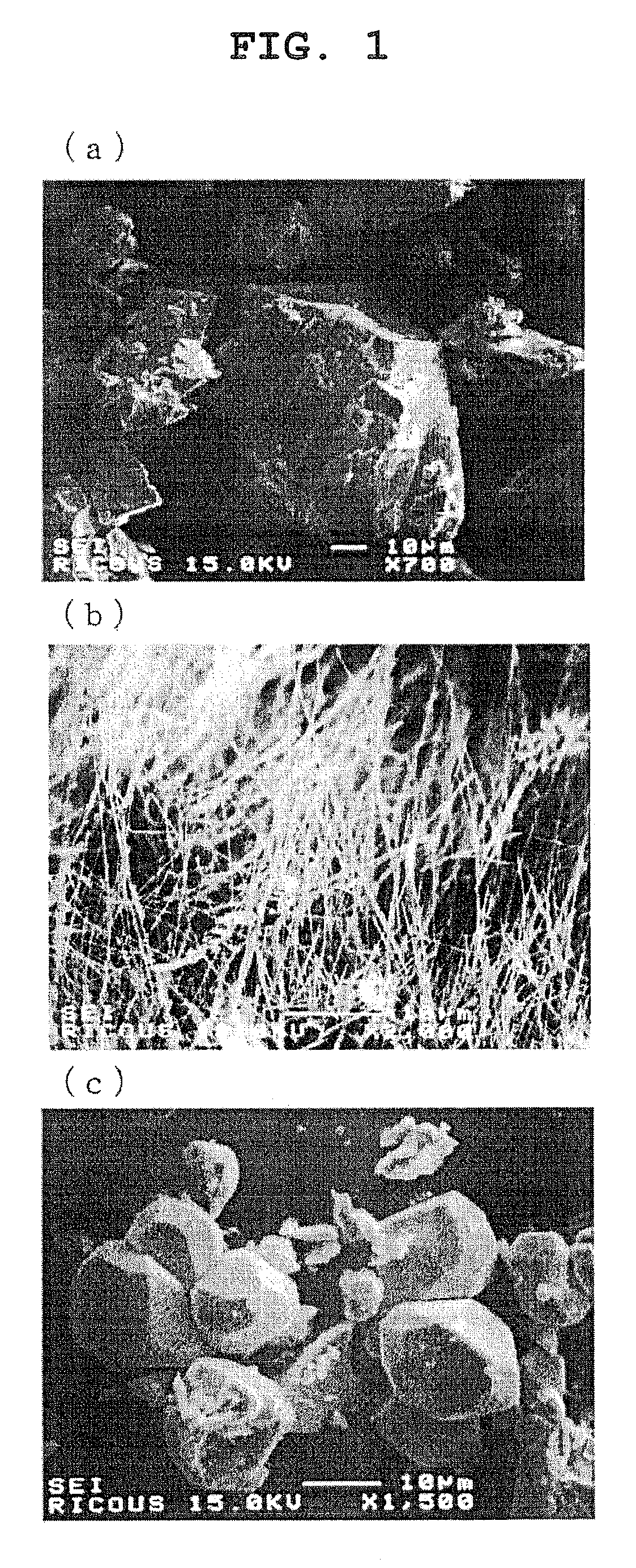
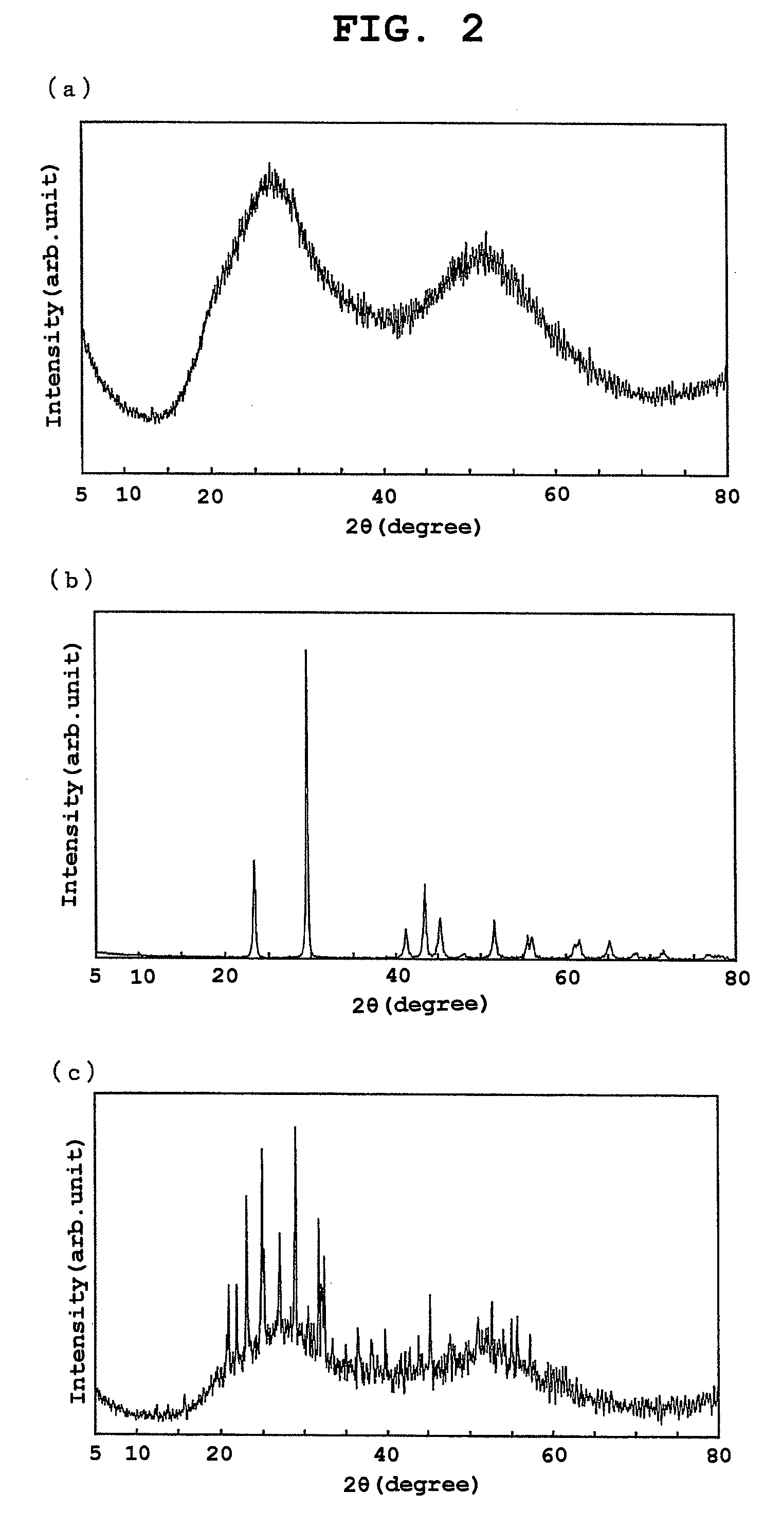
[0087]A commercially available granular amorphous selenium (purity: 99.9999%, Rare Metallic Co., Ltd.) was milled into a fine powder in a mortar. The granulated amorphous selenium was irregular particles having a particle size of 20-30 μm. This amorphous selenium fine powder (about 0.3 g) was added to acetone (7 mL, relative permittivity: 20.7) in a glass tube, and the mixture was left standing at room temperature for 10 days. In addition, similarly, an amorphous selenium fine powder (about 0.3 g) was added to benzene (7 mL, relative permittivity: 2.3) in a glass tube, and the mixture was left standing at room temperature for 10 days.

[0088]The form of the amorphous selenium fine powder, the resultant product in acetone and the resultant product in benzene was observed with a scanning electron microscope (SEM, JOEL JXA-8900). In addition, the crystal structures thereof were analyzed by an X-ray diffraction apparatus (manufactured by Rigaku Corporation, RINT 2500).

[0089]FIG. 1(a) is a...

example 2

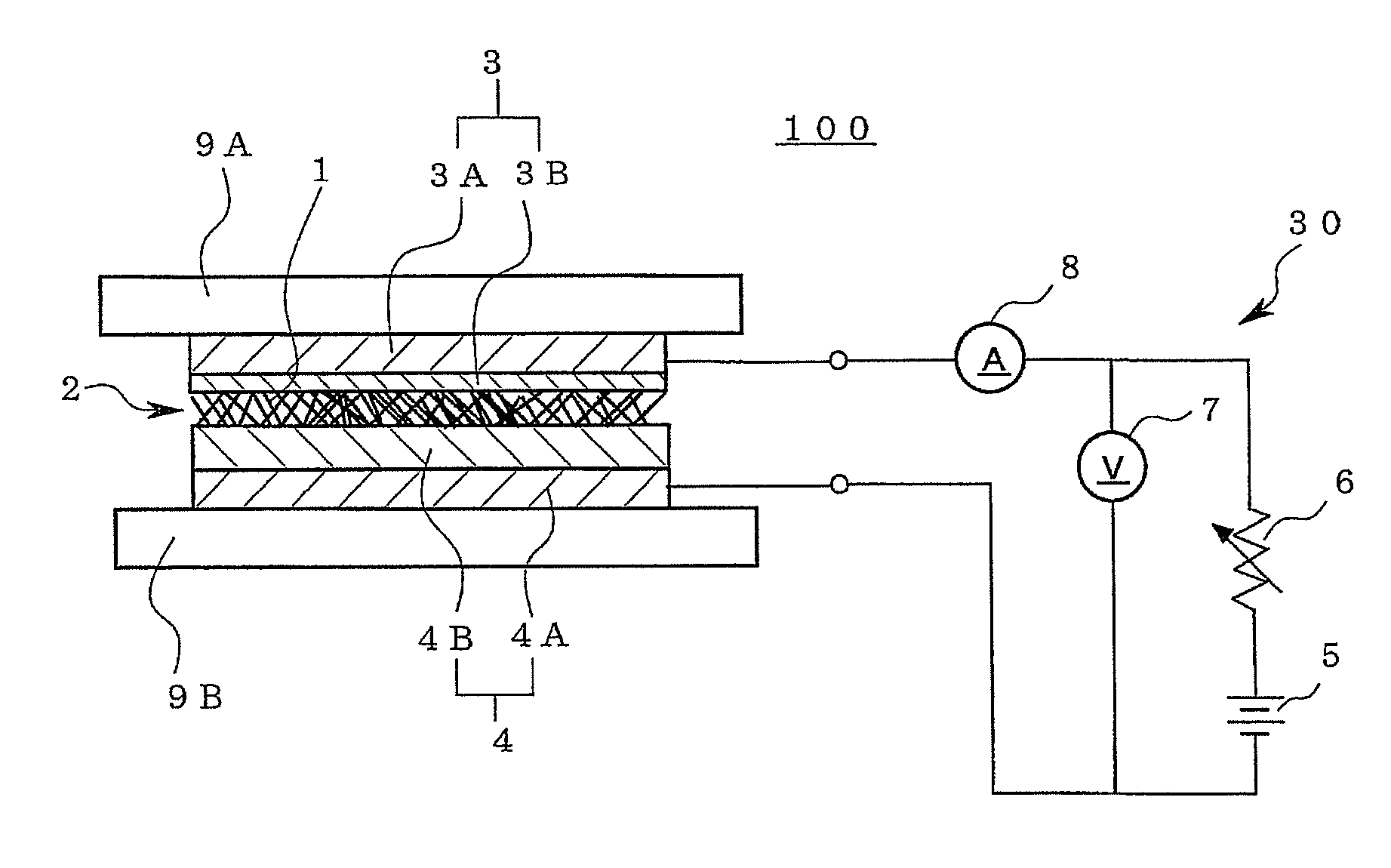
[0092]A gas sensor shown in FIG. 4 was produced using the selenium nanowire (nanowire hexagonal microcrystalline selenium with thickness 258 nm and length 4.3 μm) and granular microcrystalline selenium (granular monoclinic microcrystalline selenium having an average particle size of about 10 μm), which were obtained in Example 1, and the amorphous selenium fine powder (ground product) used in Example 1.

[0093]That is, an ultratrace amount (about 50 μg) of a selenium nanowire was uniformly adsorbed on one surface of a carbon tape (length×width×thickness of 1.0 mm×1.0 mm×0.16 mm, manufactured by Nisshin EM Corporation, carbon double-faced adhesive tape) with a wooden extra fine stick. The thickness of the carbon tape after adsorption of the selenium nanowire was about 75 μm, and that of a selenium nanowire adsorption layer was 23 μm. The selenium nanowire was weighed with Sartorius Basic plus balance BP221S manufactured by SARTORIUS K.K. One surface of the carbon tape, which is on the ...

experimental example 1

[0099]Using the gas sensor apparatus prepared above, an organic gas was contacted with a gas detector part through which an electric current was flown at room temperature and fixed voltage 5V, and current value change (I / I0) due to the organic gas were examined. Here, I0 is a constant current value before contacting the organic gas with the gas detector part, and I is a current value after contacting the organic gas with the gas detector part. As the organic gas, acetone and benzene were used, and the organic gas was contacted with the gas detector part by impregnating a cotton swab with the organic solvent (acetone, benzene), bringing the cotton swab near to the gas detector part, and allowing contact of each gas (acetone 5400 ppm, benzene 220 ppm) volatilized from the cotton swab with the gas detector part for 120 seconds. The concentration of the organic gas was measured by a gas detector tube manufactured by GASTEC CORPORATION. The method including impregnating a cotton swab wit...


PUM

PropertyMeasurementUnit
thicknessaaaaaaaaaa
particle sizeaaaaaaaaaa
relative permittivityaaaaaaaaaa

Abstract

The invention provides a gas sensitive material made from microcrystalline selenium (preferably selenium nanowire) and a gas sensor having an element structure wherein the gas sensitive material is disposed between two electrodes.The invention allows for the kind of organic gas to be distinguished, because microcrystalline selenium reacts with organic gas molecules with high sensitivity at room temperature without being influenced by humidity, and the magnitude of change of the value of the current flowing at a fixed voltage varies depending on the kind of an organic gas to be sensed.

Description

CROSS-REFERENCE TO RELATED APPLICATIONS[0001]This patent application is a U.S. National Phase of PCT / JP2010 / 069614, filed Nov. 4, 2010, which claims the benefit of Japanese Patent Application No. 2009-254461, filed Nov. 5, 2009, which is incorporated by reference.TECHNICAL FIELD[0002]The present invention relates to a gas sensitive material comprising microcrystalline selenium and a novel gas detection technique comprising detecting a gas (particularly organic gas) by using the gas sensitive material.BACKGROUND ART[0003]In recent years, detection of gas in the environment has become increasingly important for avoidance of danger caused by noxious gas, odorless carbon monoxide gas and the like in the environment. As a gas sensor for detection of such gas in the environment, semiconductor type gas sensors are conventionally known (e.g., patent document 1). This gas sensor is a P-N type gas sensor that electrically detects resistance value that changes when N-type semiconductor and P-t...

Claims


Application Information

Patent Timeline
Patent Type & Authority Patents(United States)
IPC IPC(8): G01N27/12
CPCG01N27/125G01N27/127G01N27/12
Inventor AKIYAMA, NORIOOHTANI, TSUKIO
Owner KAKE EDUCATIONAL INSTITUTION
Why Eureka
Try Eureka