Check patentability & draft patents in minutes with Patsnap Eureka AI!

Semiconductor ceramic and method for manufacturing the same, and laminated semiconductor ceramic capacitor with varistor function and method for manufacturing the same

a semiconductor ceramic and varistor technology, applied in the direction of fixed capacitors, non-conductive materials with dispersed conductive materials, solid-state devices, etc., can solve the problems of capacitor itself being broken, semiconductor elements to be broken, capacitors themselves not functioning to absorb high-voltage pulses or static electricity, etc., to suppress the variation in characteristics between products, high efficiency, stable characteristics

Inactive Publication Date: 2015-10-06
MURATA MFG CO LTD
View PDF17 Cites 0 Cited by
  • Summary
  • Abstract
  • Description
  • Claims
  • Application Information

AI Technical Summary

Benefits of technology

This approach results in a highly reliable laminated semiconductor ceramic capacitor with stable varistor characteristics and enhanced ESD withstand voltage, capable of replacing both capacitors and zener diodes, reducing component count and facilitating design standardization while enabling mass production.

Problems solved by technology

However, while these capacitors deliver superior performance on the absorption of high-frequency noises, the capacitors themselves do not function to absorb high-voltage pulses or static electricity.
For this reason, there is a possibility that the high-voltage pulses or static electricity may cause the electronic device to malfunction or cause the semiconductor elements to be broken if high-voltage pulses or static electricity are input to the electronic devices.
Particularly, when the capacitor has a low capacitance on the order of 1 nF, there is a possibility that this may cause the capacitor itself to be broken since an ESD (electro-static discharge) withstand voltage is extremely low (for example, about 2 to 4 kV).
However, when the zener diode 105 is disposed in parallel to the bypass capacitor 104 as described above, the number of components is increased to cause an increase in cost, and moreover, space for the placement of the components has to be secured, and there is thus a possibility that an increase in the size of the device may result.

Method used

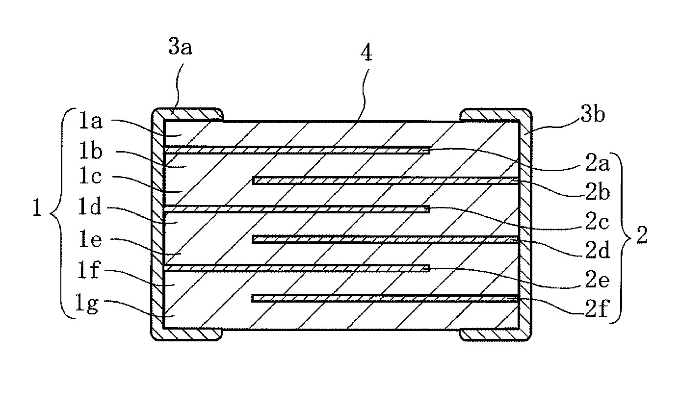
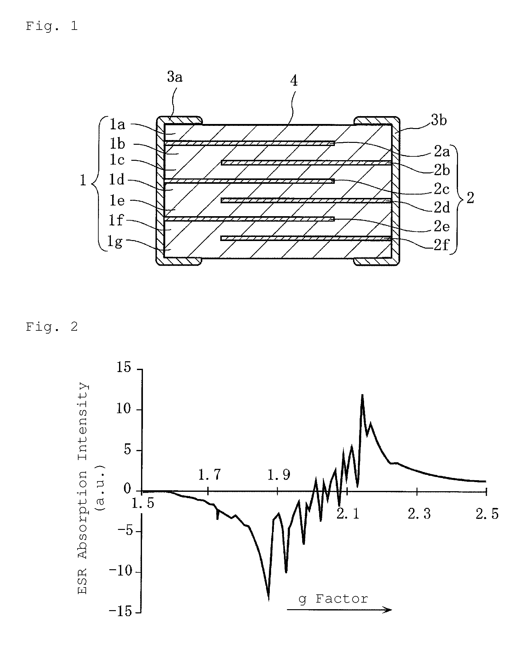
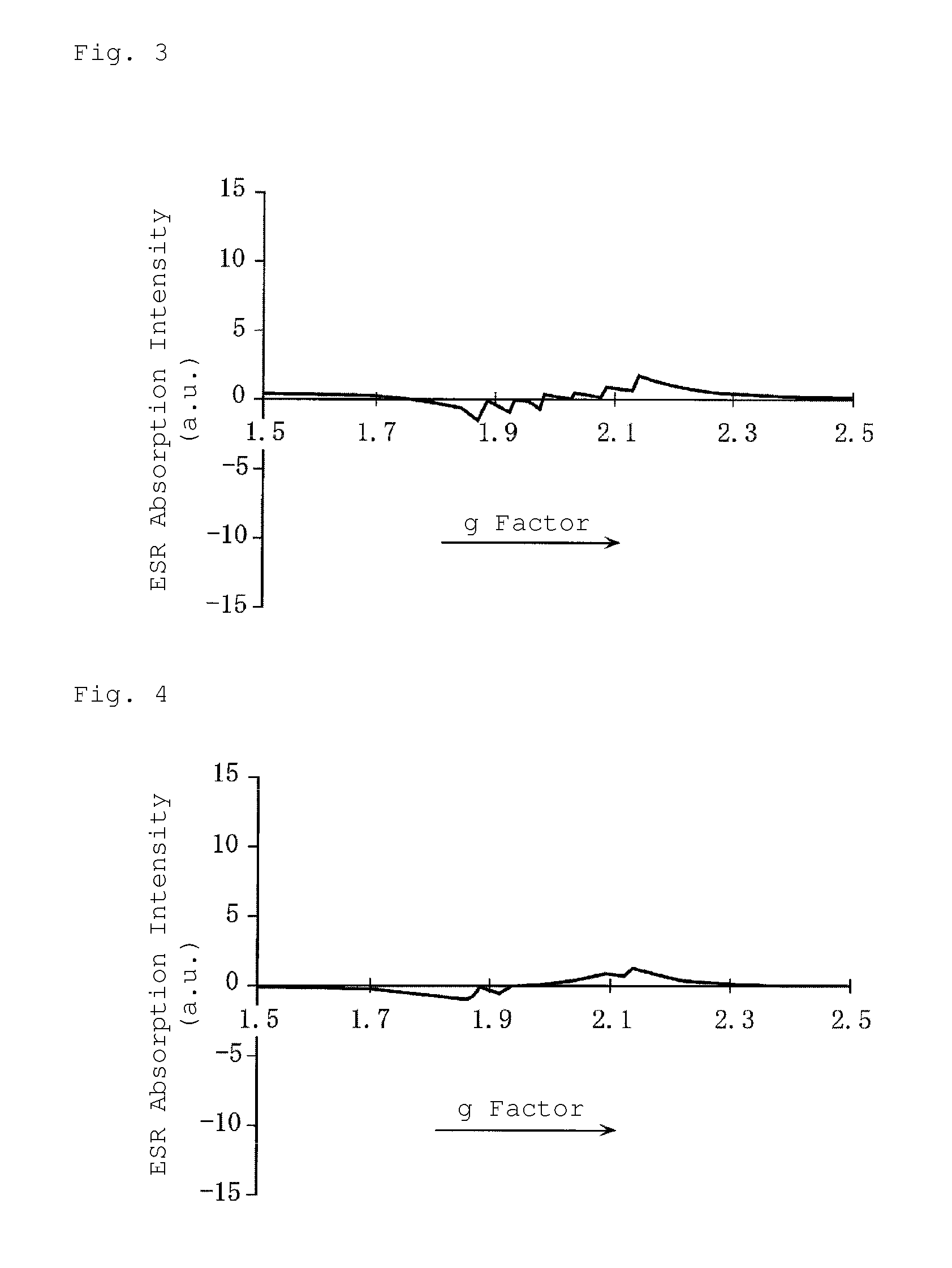

Image

  • Semiconductor ceramic and method for manufacturing the same, and laminated semiconductor ceramic capacitor with varistor function and method for manufacturing the same
  • Semiconductor ceramic and method for manufacturing the same, and laminated semiconductor ceramic capacitor with varistor function and method for manufacturing the same
  • Semiconductor ceramic and method for manufacturing the same, and laminated semiconductor ceramic capacitor with varistor function and method for manufacturing the same

Examples


examples

Preparation of Sample

Sample No. 1

[0111]As ceramic raw materials, SrCO3, TiO2 having a specific surface area of 30 m2 / g (average grain diameter: about 30 nm), and LaCl3 as a donor compound were prepared. Then, LaCl3 was weighed in such a way that the content of La was 0.8 mol with respect to 100 mol of the Ti element, and further SrO3 and TiO2 were weighed in such a way that the compounding molar ratio m of a Sr site to a Ti site (=Sr site / Ti site) was 1.000.

[0112]Three parts by weight of ammonium polycarboxylate were added to 100 parts by weight of these weighed materials as a dispersant, and then the resulting mixture was charged into a ball mill with PSZ balls of 2 mm in diameter as a pulverizing medium and pure water, and subjected to wet mixing for 16 hours in the ball mill to prepare a slurry.

[0113]Next, this slurry was evaporated to dryness, and then subjected to a calcination treatment at a temperature of 1400° C. for 2 hours in the atmosphere of the air to obtain a calcined ...


PUM

PropertyMeasurementUnit
molar ratioaaaaaaaaaa
capacitanceaaaaaaaaaa
grain diameteraaaaaaaaaa

Abstract

A semiconductor ceramic contains a donor element solid-solved in crystal grains of a SrTiO3-based compound, and an acceptor element in a grain boundary layer. The number of tetravalent acceptor elements is 1×10¹⁷ / g or more, as determined from an electron spin resonance absorption spectrum. A mixture of a calcined powder and an acceptor compound is pulverized to a specific surface area of 5.0 to 7.5 m2 / g before mixing with a binder. Semiconductor ceramic layers having a varistor function are formed by using the semiconductor ceramic forming a highly reliable capacitor which can suppress characteristics variations to stably obtain good electrical characteristics.

Description

[0001]This is a continuation of application Serial No. PCT / JP2012 / 051778, filed Jan. 27, 2012, the entire contents of which are incorporated herein by reference.TECHNICAL FIELD[0002]The present invention relates to a semiconductor ceramic and a method for manufacturing the same, and a laminated semiconductor ceramic capacitor with a varistor function and a method for manufacturing the same, and more specifically to a SrTiO3-based grain boundary insulated semiconductor ceramic, a method for manufacturing the semiconductor ceramic, a laminated semiconductor ceramic capacitor with a varistor function using the semiconductor ceramic, and a method for manufacturing the same.BACKGROUND ART[0003]In recent years, mobile electronic devices such as cellular phones and laptop personal computers, and in-car electronic devices to be installed on cars have become common with the development of electronics technology, and a reduction in size with multi-functionalization has been required for the e...

Claims


Application Information

Patent Timeline
Patent Type & Authority Patents(United States)
IPC IPC(8): C04B35/465C04B35/47H01L49/02H01G4/10H01G4/12H01G4/30B28B11/24C01G23/00B82Y30/00C04B35/626H10N97/00
CPCC04B35/47C04B35/6261H01G4/1227H01G4/30H01L28/60B28B11/24B82Y30/00C01G23/006C01P2006/12C01P2006/40C04B2235/3224C04B2235/3227C04B2235/3241C04B2235/3251C04B2235/3258C04B2235/3262C04B2235/3275C04B2235/3279C04B2235/3281C04B2235/3418C04B2235/36C04B2235/441C04B2235/444C04B2235/483C04B2235/5409C04B2235/5454C04B2235/652C04B2235/6582C04B2235/663C04B2235/786C04B2235/79C04B2235/85
Inventor KAWAMOTO, MITSUTOSHI
Owner MURATA MFG CO LTD
Features
  • R&D
  • Intellectual Property
  • Life Sciences
  • Materials
  • Tech Scout
  • Unparalleled Data Quality
  • Higher Quality Content
  • 60% Fewer Hallucinations
Learn More