Transparent electrically conducting oxides

a technology of electrical conductivity and oxides, applied in the direction of liquid/solution decomposition chemical coatings, non-metal conductors, instruments, etc., can solve the problems of limited application range of pld in the industry, difficult to sustain stable supply of indium for an expanding market of flat panel displays, solar cells, etc., and achieves low cost, convenient large-area deposition, and low cost

Active Publication Date: 2016-01-12
OXFORD UNIV INNOVATION LTD
View PDF118 Cites 3 Cited by
  • Summary
  • Abstract
  • Description
  • Claims
  • Application Information

AI Technical Summary

Benefits of technology

[0015]The present inventors have provided an improved process for producing a transparent conducting film of a silicon-doped zinc oxide. Such films have temperature-stable electrical and optical properties which are comparable to those of ITO. The process, which typically involves the deposition of a liquid or gel precursor onto a heated substrate, is advantageous on account of its low cost, its convenience for large-area deposition, its convenience for deposition over curved and / or non-uniform surface topologies, and its simplicity: the deposition and doping steps can effectively be carried out simultaneously. Furthermore, unlike PLD deposition, the process does not require a vacuum system or an expensive excimer laser. The process is therefore inexpensive, and can be performed in ambient conditions (ambient pressure and, aside from heating the substrate, at ambient temperature). The process is therefore easy to handle, inexpensive, suitable for industrial use, and can be used to produce large-area thin films of the transparent conducting oxide. Accordingly, the inventors have devised a new, low-cost method for the effective doping of ZnO with silicon using liquid precursor solutions, which enables the preparation of large area transparent conducting silicon-doped ZnO thin films. The process offers significant economic advantages relative to capital-intensive vapour-phase deposition methods.
[0016]Since the films can be made to cover a wide surface area, and since the cost of making ZnO is very low, the films of the invention are particularly attractive for large scale applications such as solid-state lighting, transparent electronics, flat-panel displays, energy-efficient windows and solar cells (particularly large-area solar cells).
[0017]The silicon-doped zinc oxide films produced by the process of the invention are attractive for transparent conductor applications as they are easy to produce from inexpensive, abundant precursors, and are non-toxic. Furthermore, silicon-doped zinc oxide has a higher visible transmittance than many other conductive oxide films and is more resistant to reduction by hydrogen-containing plasma processes that are commonly used for the production of solar cells. Zinc oxide itself is also inexpensive, abundant in nature and non-toxic. It also has certain properties which are considered important for transparent conductors, such as a band gap of 3.4 eV, an intrinsic carrier concentration of about 1016 cm−3 and an electron Hall mobility of 200 cm2V−1s−1. By using the process of the invention, large-area silicon-doped zinc oxide films can be produced.

Problems solved by technology

Due to the cost and scarcity of indium metal, the principle component of ITO, a stable supply of indium may be difficult to sustain for an expanding market for flat panel displays, solar cells, printed electronics and other applications.
Although PLD is a very useful tool for the growth of oxides (and other chemically complex systems) by reactive deposition, and allows key research to be performed in exploratory chemical doping programmes, PLD has limited applicability in industry and has certain drawbacks.
Furthermore, the nature of the PLD apparatus and process restricts the size of the substrate on which the film is deposited and, in turn, the coverage area of film that can be deposited on a substrate.
Furthermore, the area of film deposition is limited by the width of the plasma plume that is produced in the PLD apparatus, and the degree to which the substrate is moveable (translatable) relative to the plume within the chamber.
Furthermore, the PLD process can lead to films with a non-uniform composition, due to the fact that the PLD ablation plume consists of two components; a high-intensity, leading part, which is usually stoichiometric in target composition, and a lower intensity non-stoichiometric material.
Additionally, both the PLD apparatus and the PLD process are expensive, requiring a vacuum system and an excimer laser.
Finally, the PLD process is usually limited to the deposition of films onto flat surfaces and materials, which restricts the types of substrates that can be coated using PLD.

Method used


Image

  • Transparent electrically conducting oxides
  • Transparent electrically conducting oxides
  • Transparent electrically conducting oxides

Examples


example 1

Preparation of Precursor Solution

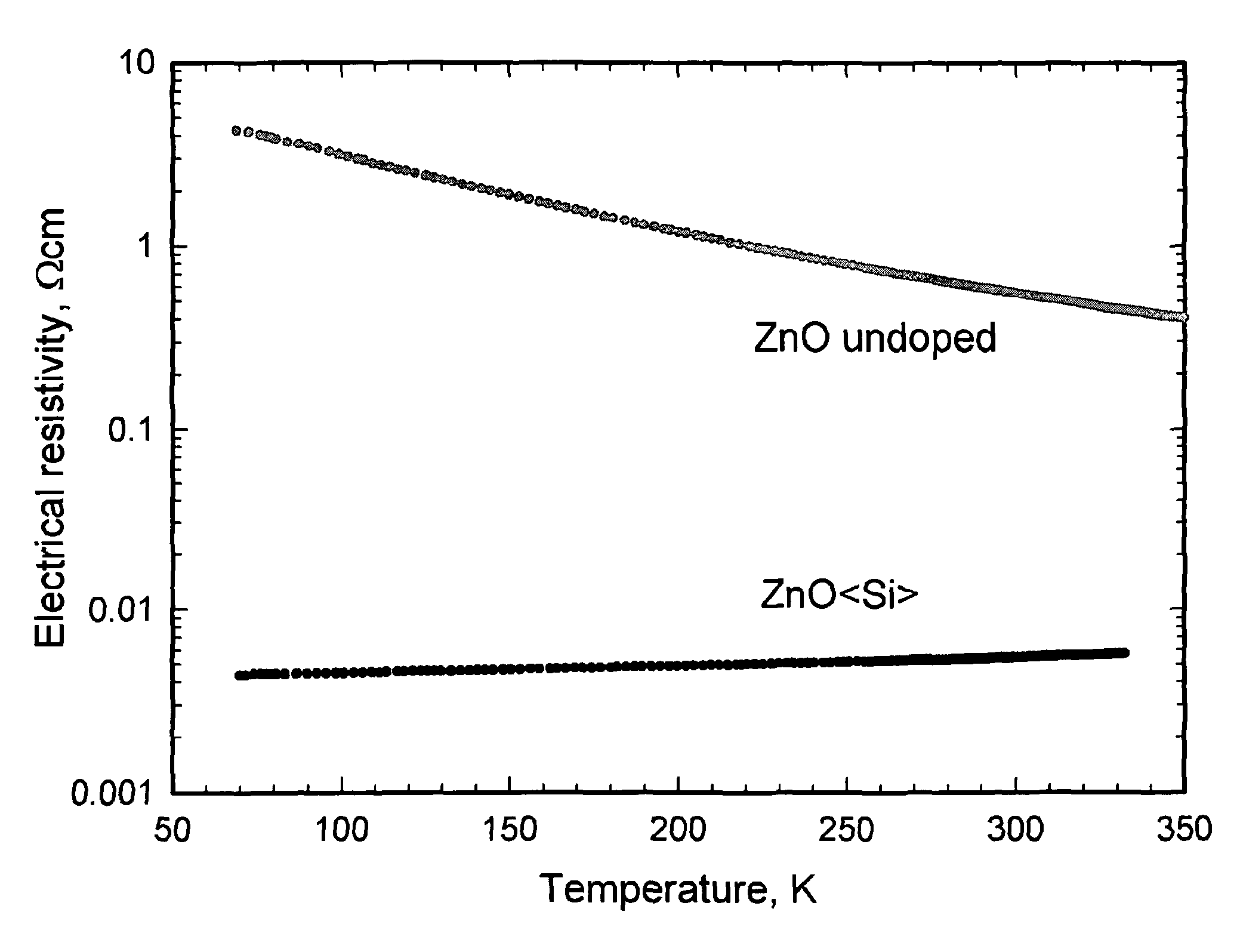
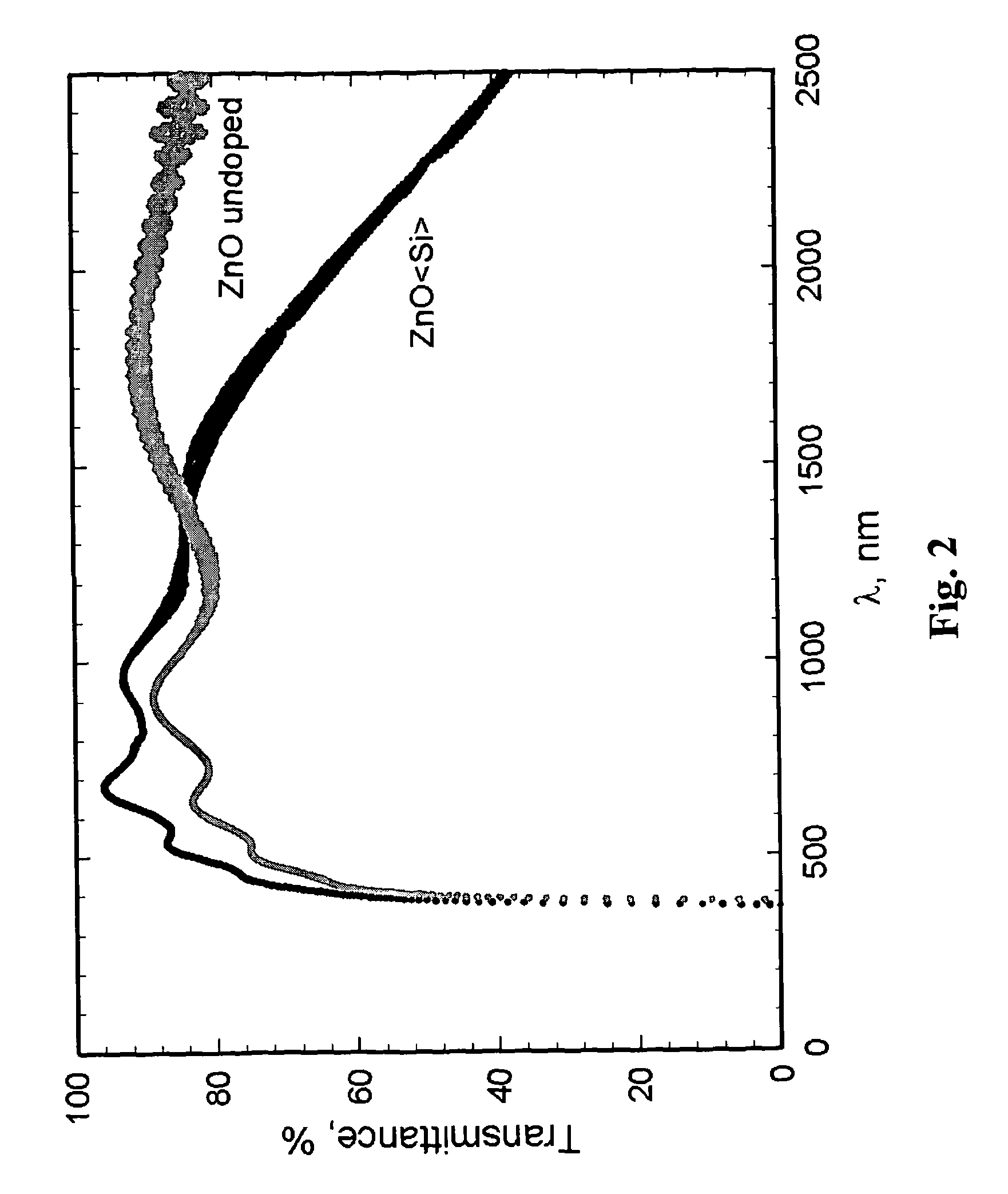
[0183]A precursor solution was prepared by mixing 17.5 ml of isopropanol, 6.75 ml of deionised water and 0.75 of concentrated acetic acid in a volumetric ratio of 70:27:3, respectively. Then, 0.0133 g of silicon tetra-acetate was completely dissolved in the solvent mixture at a temperature of 50° C. Subsequently, 0.4585 g of zinc acetate dihydrate was dissolved in the resulting solution. The concentration of zinc acetate in the final precursor solution was 0.1 M, and the concentration of silicon tetra-acetate in the final precursor solution was 0.002 M, thereby giving a Si / (Si+Zn) ratio of about 0.02 (i.e. 2 mol % Si). These masses and volumes enable preparation of 25 ml of precursor solution, which is typically used for depositing thin films of around 3-4 cm2. Larger area films may be prepared using larger volumes of precursor solution, as described below in Example 2.

Deposition of a Silicon-doped Zinc Oxide Thin Film by Spray Pyrolysis

[0184]The pre...

example 2

Preparation of a Larger Volume of Precursor Solution, for Deposition of a Film Over a Surface Area of 0.01 m2

[0190]A precursor solution is prepared by mixing 437.5 ml of isopropanol, 168.75 ml of deionised water and 18.75 ml of concentrated acetic acid in a volumetric ratio of 70:27:3, respectively. Then, 0.3325 g of silicon tetra-acetate is completely dissolved in the solvent mixture at a temperature of 50° C. Subsequently, 11.4625 g of zinc acetate dihydrate is dissolved in the resulting solution. The concentration of zinc acetate in the final precursor solution is 0.1 M, and the concentration of silicon tetra-acetate in the final precursor solution is 0.002 M, thereby giving a Si / (Si+Zn) ratio of about 0.02 (i.e. 2 mol % Si).

[0191]The precursor solution may then be deposited, using spray pyrolysis as disclosed in Example 1, to form a Si-doped ZnO thin film as described in Example 1, over an area of 0.01 m2.

[0192]Even larger area thin films may be prepared by scaling-up the volum...


PUM

PropertyMeasurementUnit
electrical resistivityaaaaaaaaaa
distanceaaaaaaaaaa
diameteraaaaaaaaaa

Abstract

The invention provides a process for producing a transparent conducting film, which film comprises a doped zinc oxide wherein the dopant comprises Si, which process comprises: disposing a composition which is a liquid composition or a gel composition onto a substrate, wherein the composition comprises Zn and Si; and heating said substrate. The invention further provides transparent conducting films obtainable by the process of the invention, including transparent conducting films which comprise a doped zinc oxide wherein the dopant comprises Si, and wherein the film covers a surface area equal to or greater than 0.01 m2. The invention also provides a coated substrate, which substrate comprises a surface, which surface is coated with a transparent conducting film, wherein the film comprises a doped zinc oxide wherein the dopant comprises Si, and wherein the area of said surface which is coated with said film is equal to or greater than 0.01 m2. The invention further provides coatings comprising the films of the invention, processes for producing such films and coatings, and various uses of the films and coatings.

Description

CROSS REFERENCE TO RELATED APPLICATIONS[0001]This application is a National Phase application under 35 U.S.C. §371 of International Application No. PCT / GB2010 / 001664, having an International Filing Date of Sep. 2, 2010, which claims priority to British Application No. GB 0915376.8 filed on Sep. 3, 2009, each of which are incorporated herein by reference in their entireties.FIELD OF THE INVENTION[0002]The invention relates to a process for producing a transparent conducting film, to transparent conducting films obtainable by that process, to coatings comprising such films, and to various uses of the films and coatings.BACKGROUND TO THE INVENTION[0003]Sn-doped In2O3 thin films [In2-xSnxO3: ITO] exhibit a remarkable combination of optical and electrical transport properties. These include a low electrical resistivity, which is typically in the order of 10−4 Ωcm. This property is related to the presence of shallow donor or impurity states located close to the host (In2O3) conduction ban...

Claims


Application Information

Patent Timeline
Patent Type & Authority Patents(United States)
IPC IPC(8): B05D5/12C23C18/08C23C18/12H01B1/08B05D3/10
CPCH01B1/08C23C18/08C23C18/1208C23C18/1216C23C18/1233C23C18/1245C23C18/1254C23C18/1258C23C18/1291C23C18/1295B05D3/10B05D5/12Y10T428/24479Y10T428/24628Y10T428/24802
Inventor KUZNETSOV, VLADIMIR L.EDWARDS, PETER P.
Owner OXFORD UNIV INNOVATION LTD
Why Eureka
Try Eureka