Method for manufacturing nitride semiconductor device

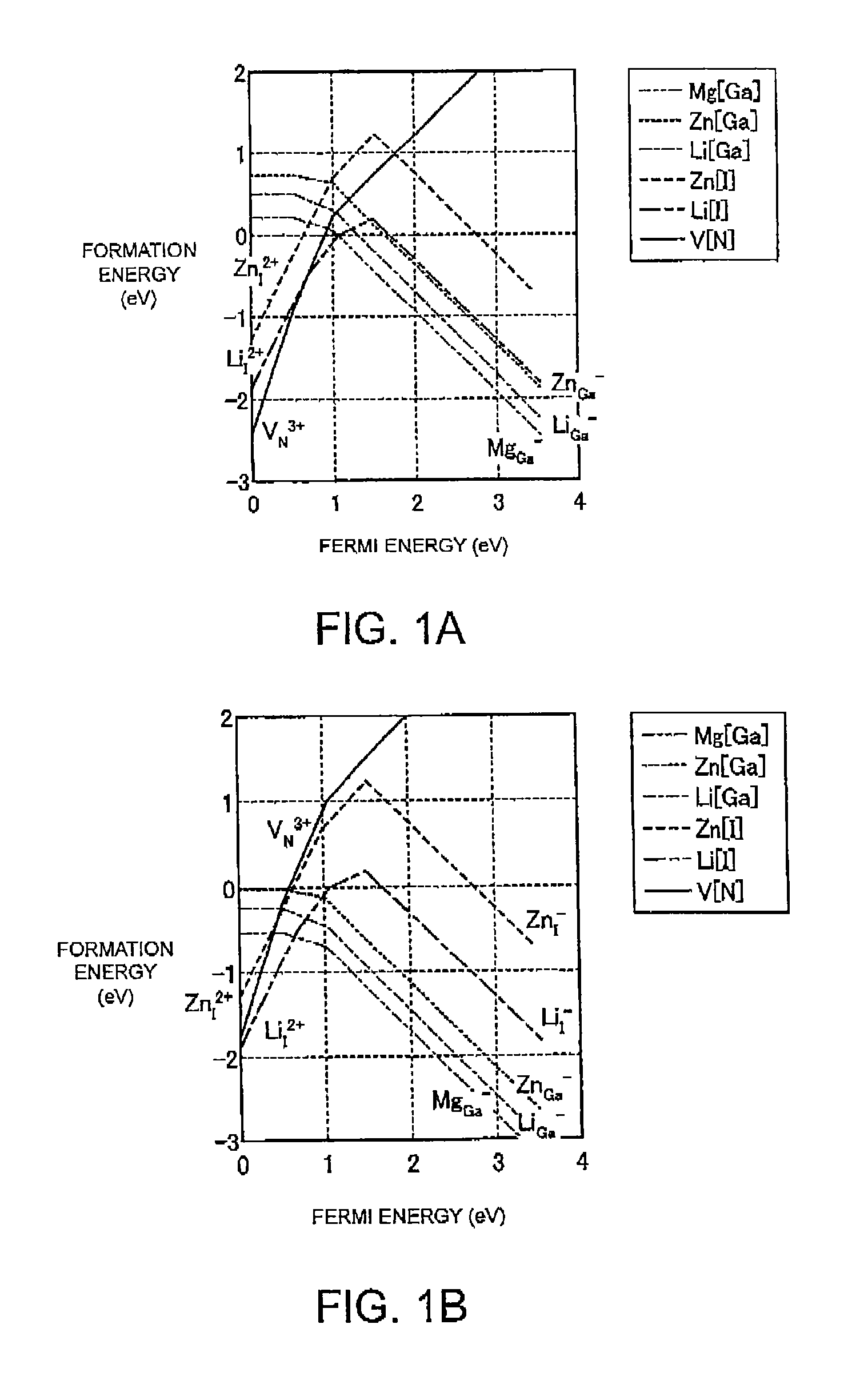
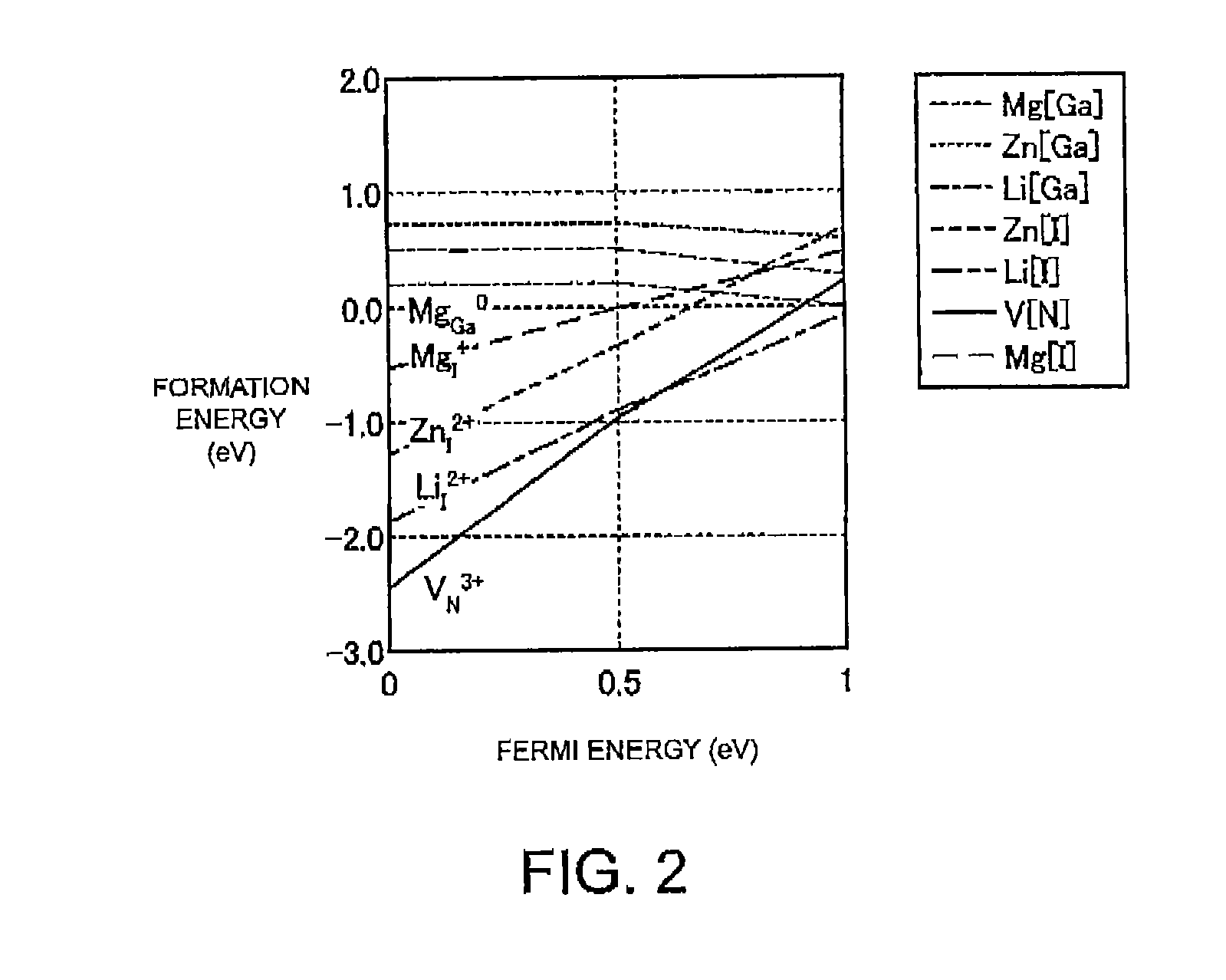
a semiconductor device and manufacturing method technology, applied in semiconductor devices, diodes, electrical devices, etc., can solve the problems of affecting the electrical characteristics of the rate is physically determined, and the mg that has entered the interstitial site is adversely affected by the mg, so as to achieve high acceptor concentration and high hole concentration

Active Publication Date: 2016-02-23
FURUKAWA ELECTRIC CO LTD
View PDF25 Cites 2 Cited by
  • Summary
  • Abstract
  • Description
  • Claims
  • Application Information

AI Technical Summary

Benefits of technology

[0025]The method for manufacturing a nitride semiconductor device according to the present invention can effectively dope magnesium of a p-type dopant and can realize a high acceptor concentration and a high hole concentration in a group III nitride semiconductor.

Problems solved by technology

However, there are concerns about safety when a malfunction occurs in the power supply circuit due to the normally-on characteristic in the AlGaN / GaN-HFET described above.
However, the ionization rate is a physically determined amount and there is no room for artificial improvements.
Mg that has entered an interstitial site adversely affects electrical characteristics due to segregation in low angle grain boundaries and threading dislocation in the crystal and on the surface.
Moreover, because Ga interstitial atoms are also formed in addition to nitrogen vacancy (VN), there are problems that bring about a current collapse phenomenon and characteristic fluctuation in the electronic device.
Therefore, realizing a p-type GaN layer that provides the quality required by an electronic device has been difficult in a GaN based electronic device.
However, formation control of this type of donor-acceptor pair is difficult, and the above method has a problem in that an n-type dopant present alone may be introduced.
Furthermore, because the deep level introduces the current collapse phenomenon, it is not suitable for electronic device applications.
Because this n-type dopant remains in GaN, it has a problem in that the element characteristics fluctuate due to external disturbances such as electrification.
However, because 1018 cm−3 or more of Zn remains in the GaN with this method, the problem of bringing about the current collapse phenomenon in the electronic device remains.
On account of this, there is a problem in that leakage current increases through the p-type GaN layer.

Method used


Image

  • Method for manufacturing nitride semiconductor device
  • Method for manufacturing nitride semiconductor device
  • Method for manufacturing nitride semiconductor device

Examples


first embodiment

[0059]First, a description will be given of a nitride semiconductor device according to a first embodiment of the present invention. FIG. 4 illustrates a vertical type rectifier (pn junction) diode as the nitride semiconductor device according to the first embodiment.

[0060]As illustrated in FIG. 4, the pa junction diode is configured by sequentially layering an n−-GaN layer 42, p-GaN layer 43, p+-GaN layer 44, and an anode electrode 4A on one main surface of an n+-GaN substrate 41, and a cathode electrode 4C is provided on another main surface of the n+-GaN substrate 41. The following is a description of a manufacturing method of the vertical type pn junction diode as configured above according to the first embodiment.

(Epitaxial Substrate Production)

[0061]First, the n+-GaN substrate 41 with a thickness of 300 μm and a 2 inch diameter having n+ conductivity is installed in an MOCVD apparatus (not illustrated). Note that, the dopant of the n+-GaN substrate 41 is Si, and the carrier co...

second embodiment

[0072]Next, a description will be given of a nitride semiconductor device according to a second embodiment of the present invention. FIG. 5 is a cross-sectional view of a pseudo-vertical type rectifier (pn junction) diode having a modified form from the first embodiment described above.

[0073]As illustrated in FIG. 5, the pseudo-vertical type pn junction diode according to the second embodiment is provided with, in order on a sapphire substrate 45, a buffer layer 46 and an n+-GaN layer 47. An n−-GaN layer 42, a p-GaN layer 43, and a p+-GaN layer 44 are sequentially provided in a section on the n+-GaN layer 47. The anode electrode 4A is provided on the p+-GaN layer 44. Further, the cathode electrode 4C is provided on the n+-GaN layer 47 in the section where the n−-GaN layer 42, the p-GaN layer 43, and the p+-GaN Layer 44 were removed. Next, the following is a description of a manufacturing method of the pseudo-vertical type pn junction diode as configured above according to the second...

third embodiment

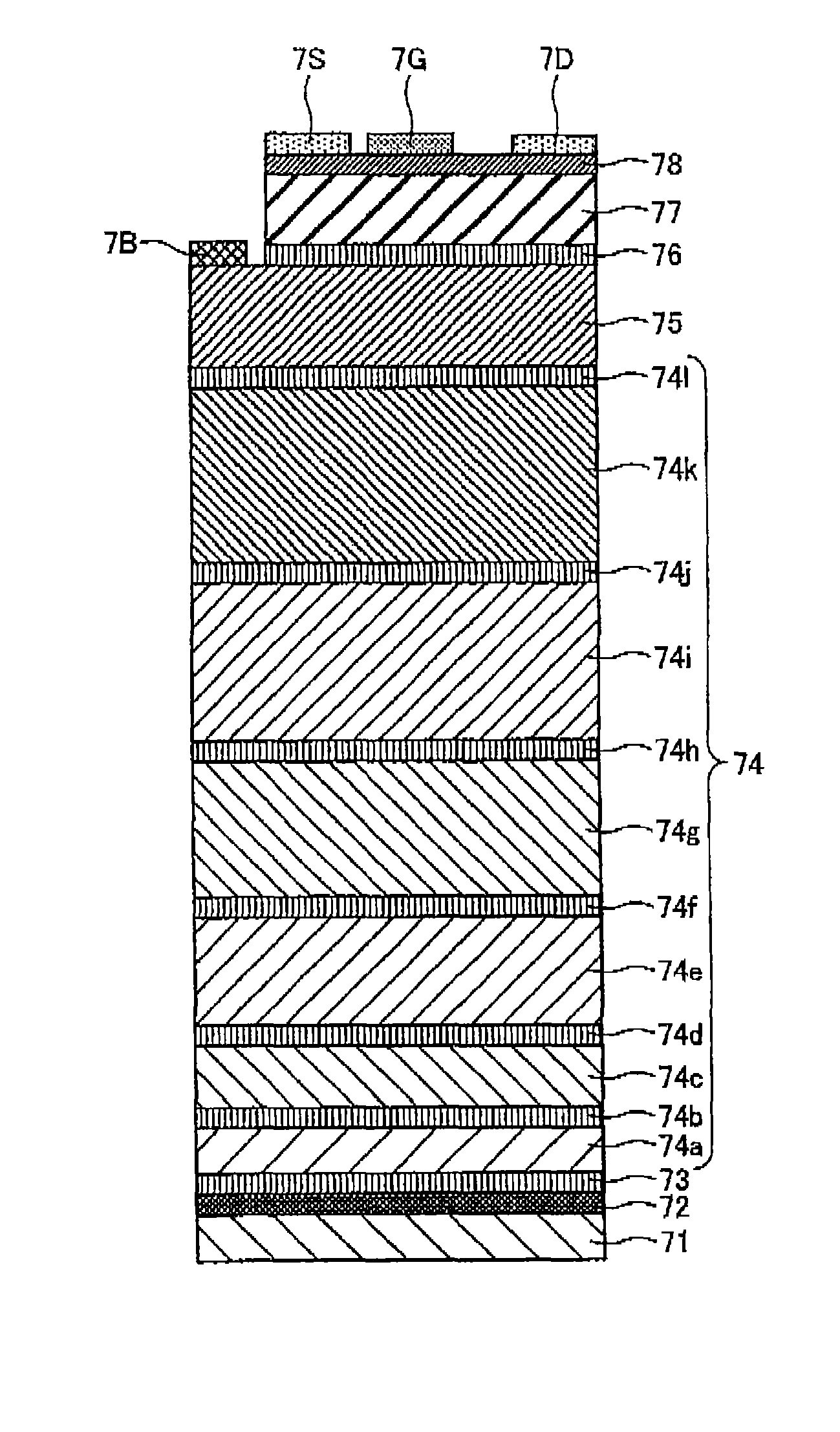
[0077]Next, a description will be given of a nitride semiconductor device according to a third embodiment of the present invention. Note that in the third embodiment to be described below, a description will be given of an example where the nitride semiconductor device is a light emitting diode, but it is not always limited to a light emitting diode and may be, for example, a laser diode or other type of light emitting device. FIG. 6 is a cross-sectional view of a light emitting diode (LED) element according to the third embodiment.

[0078]As illustrated in FIG. 6, in the LED element according to the third embodiment is provided with, in order on a sapphire substrate 51, a buffer layer 52 and an n+-GaN layer 53. An n-GaN cladding layer 54, active layer 55, p-GaN cladding layer 56, and a p+-GaN layer 57 are sequentially provided in a section on an n+-GaN layer 53. An anode electrode 5A is provided on the p+-GaN layer 57.

[0079]Further, a cathode electrode 5C is provided on the n+-GaN la...


PUM

PropertyMeasurementUnit
hole concentrationaaaaaaaaaa

Abstract

Forming a group III nitride semiconductor layer having p-type conductivity on at least one layer or more formed on an Si substrate or sapphire substrate using at least one of an epitaxial growth or ion implantation method. When forming the group III nitride semiconductor layer, at least one type of metal element selected from Zn, Li, Au, Ag, Cu, Pt, and Pd having a formation energy of a group III element substitute higher than that of Mg is doped simultaneously with Mg of a p-type dopant to introduce an interstitial site. Subsequent to activation of Mg as an acceptor, the metal element is removed from the group III nitride semiconductor layer, and the concentration of the metal element is not more than 1 / 100 of the concentration of Mg to realize a hole concentration of not less than 1018 to 1019 cm−3.

Description

BACKGROUND[0001]1. Technical Field[0002]The present invention relates to a method for manufacturing a nitride semiconductor device, such as a light emitting element or an electronic device that uses a group III nitride semiconductor having a p-type conductivity.[0003]2. Background Art[0004]A group III nitride semiconductor is primarily a gallium nitride (GaN), aluminum nitride (AlN), indium nitride (InN), or a mixed crystal of these.[0005]This nitride semiconductor is used in light emitting diodes (LED), laser diodes (LD), and other light emitting devices, as well as in Schottky barrier diodes (SBD), field effect transistors (FET), and other electronic devices for power device applications.[0006]n-type and p-type conductivity control is possible with these types of nitride semiconductors when using silicon (Si) or magnesium (Mg) as a dopant. Specifically, a desired emission can be obtained by forming a pn junction in a light emitting device and implanting electrons and holes in a qu...

Claims


Application Information

Patent Timeline
Patent Type & Authority Patents(United States)
IPC IPC(8): H01L21/20H01L33/00H01L29/778H01L29/861H01L29/207H01L21/02H01L21/36H01L29/66H01L29/20
CPCH01L21/02664H01L21/0242H01L21/0254H01L21/0262H01L21/02381H01L21/02389H01L21/02458H01L21/02576H01L21/02579H01L21/02581H01L29/207H01L29/66204H01L29/66462H01L29/7787H01L29/861H01L33/007H01L29/2003
Inventor IWAMI, MASAYUKI
Owner FURUKAWA ELECTRIC CO LTD
Why Eureka
Try Eureka