Device having improved radiation hardness and high breakdown voltages

a radiation hardness and high breakdown voltage technology, applied in the direction of semiconductor devices, electrical apparatus, transistors, etc., can solve the problems of unfavorable ionizing radiation tolerance of unintended active parasitic devices being turned, and mos circuits formed using locos processes are not tolerant of ionizing radiation, so as to improve the radiation hardness of mos devices, improve the breakdown voltage, and reduce the effect of circuit density or additional complexity design impa

Active Publication Date: 2016-03-08
TEXAS INSTR INC
View PDF6 Cites 5 Cited by
  • Summary
  • Abstract
  • Description
  • Claims
  • Application Information

AI Technical Summary

Benefits of technology

[0008]These and other problems associated with the prior art are addressed by the present invention, which provides MOS devices having improved radiation hardness by separating the source and drain regions from the Bird's Beak region to eliminate radiation-induced leakage along the Bird's Beak leakage path between the source and drain regions while retaining a high breakdown voltage, and methods of fabricating these devices and integrated circuits incorporating them. This is accomplished by separating the source and drain regions from the Bird's Beak regions, specifically in the areas underlying where gate lines would cross the Bird's Beak region, which by pulling back the source and drain from the edge of the Bird's Beak into the moat region to increase the breakdown voltage while retaining a predetermined electrical width.
[0009]The present invention can be used to improve the radiation hardness of NMOS, CMOS, or BiCMOS integrated circuits produced using variations of a LOCOS technology. Digital, analog, or mixed-signal circuits can be implemented using the devices and processes provided herein. Devices produced in accordance with the present invention operate at speeds and current levels comparable to conventional unmodified NMOS transistors, while having a minimal impact on transistor size and thus circuit density. Breakdown voltages are maintained or even improved, thus allowing high voltage operation of circuits produced in accordance with the present invention.

Problems solved by technology

Among the typical issues which must be addressed is the leakage of unintended active parasitic devices turned on by voltage in interconnect lines over the field oxide, which can occur at voltages close to the operating voltage if the doping concentration is low underneath the field oxide.
It is also well known that MOS circuits formed using a LOCOS process are not tolerant of ionizing radiation such as may be encountered in space, in nuclear power plants, in medical applications or treatments involving radiation exposure such as CT scans or in the vicinity of a nuclear explosion.
When a MOS device is exposed to ionizing radiation, electron-hole pairs are generated in the various oxide regions, resulting in trapped charge and interface states.
Due to the materials involved, the effect is a cumulative buildup of positive charge in the oxide, leading to large negative threshold shifts and thus to leakage particularly in parasitic devices associated with NMOS transistors.
This leakage leads at least to increased power dissipation, and in a worst case can lead to a failure of operation of the device that incorporates the NMOS transistor.
Increasing the doping of the channel stop to preclude the possibility of radiation-induced inversion layers extending between devices can result in unacceptably low drain-to-substrate breakdown voltages in conventional designs in which the p-type channel stop abuts the n-type source and drain regions.
Moreover, pulling the channel stop away from the moat region to increase breakdown voltage further decreases the dopant concentration in the Bird's Beak region and the channel region under the gate, leading to increased source-to-drain leakage from these two paths.
Solutions to prevent parasitic leakages between and within devices by simply using higher doping to increase threshold voltages result in decreased breakdown voltages.
Hence, these designs face tradeoffs and are typically significantly larger and / or slower than the unmodified devices.

Method used


Image

  • Device having improved radiation hardness and high breakdown voltages
  • Device having improved radiation hardness and high breakdown voltages
  • Device having improved radiation hardness and high breakdown voltages

Examples


Embodiment Construction

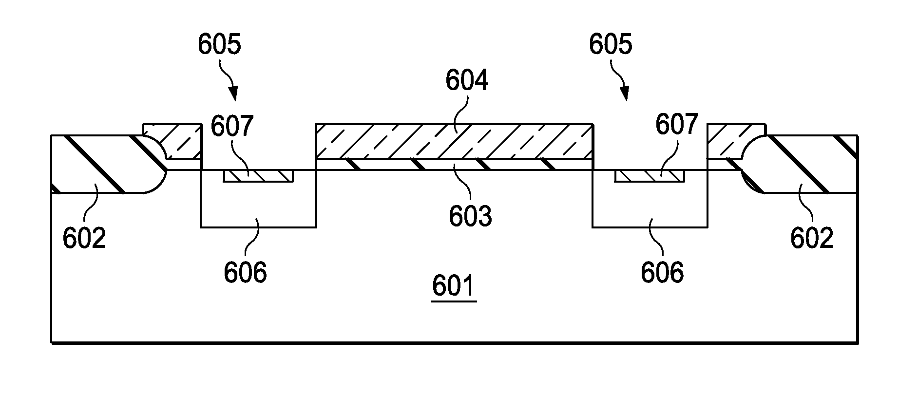
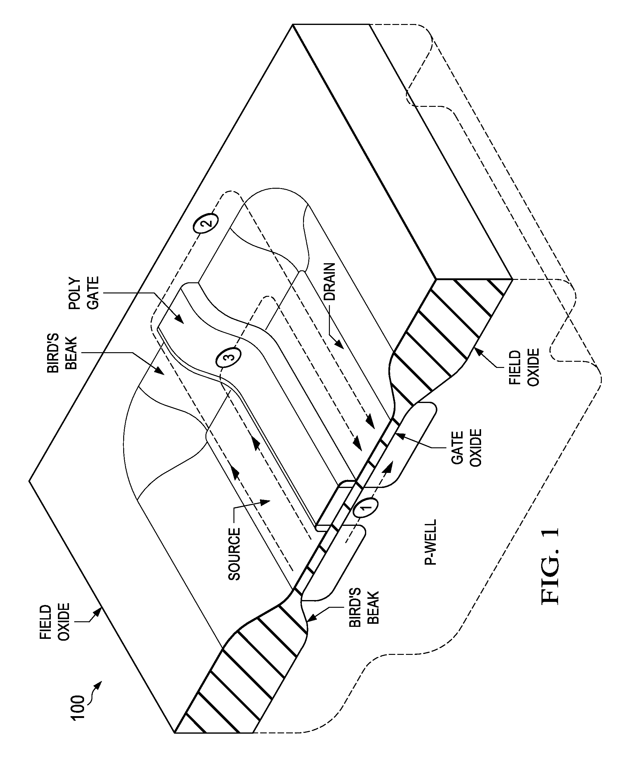
[0031]Referring to FIG. 1, there is shown a cross-sectioned isometric view of a typical NMOS transistor device 100 which can be part of an integrated circuit having multiple such transistors such as an NMOS device, a CMOS device (the PMOS transistor not being shown), or a BiCMOS device (which would additionally include bipolar junction transistors. In the illustrated device, the NMOS transistor is formed in a “p-well” which is a lightly doped p-type region formed within a silicon substrate. Alternatively, an entire top layer several micrometers thick or more of the silicon substrate can be lightly doped p-type material. The device 100 as illustrated in FIG. 1 is typical of one produced using a local oxidation of silicon (LOCOS) process used for isolating devices. It can be seen that a source and drain region are formed within a so-called “moat region” covered by a thin gate oxide, and surrounded by an isolating field oxide. Typical thicknesses for these oxides are in the range of 75...


PUM


Abstract

Radiation hardened NMOS devices suitable for application in NMOS, CMOS, or BiCMOS integrated circuits, and methods for fabricating them. A device includes a p-type silicon substrate, a field oxide surrounding a moat region on the substrate tapering through a Bird's Beak region to a gate oxide within the moat region, a heavily-doped p-type guard region underlying at least a portion of the Bird's Beak region and terminating at the inner edge of the Bird's Beak region, a gate included in the moat region, and n-type source and drain regions spaced by a gap from the inner edge of the Bird's Beak and guard regions. A variation of minor alterations to the conventional moat and n-type source / drain masks. The resulting devices have improved radiation tolerance while having a high breakdown voltage and minimal impact on circuit density.

Description

CROSS-REFERENCE TO RELATED APPLICATIONS[0001]This application claims the benefit of priority under U.S.C. §119(e) of U.S. Provisional Application 61 / 893,579 (filed Oct. 21, 2013).FIELD OF THE INVENTION[0002]The present invention relates generally to the field of semiconductor device manufacturing, and more particularly, to variations on the local oxidation of silicon process for isolation of NMOS transistors in integrated circuits having improved radiation hardness and high breakdown voltages.[0003]Local oxidation of silicon (LOCOS) fabrication processes are used to provide electrical isolation between devices in integrated circuits (ICs). Variations of such processes are known by several names and may be used to fabricate complementary metal oxide semiconductor (CMOS) as well as n-type metal oxide semiconductor (NMOS) circuits and CMOS circuits incorporating bipolar junction transistors (BiCMOS). In these processes, a thick field oxide is thermally grown in isolation regions betwee...

Claims


Application Information

Patent Timeline
Patent Type & Authority Patents(United States)
IPC IPC(8): H01L29/00H01L29/78H01L27/06H01L29/06H01L21/761H01L21/762H01L27/118H01L27/092
CPCH01L27/092H01L29/7833H01L27/0623H01L29/0646H01L29/0653H01L21/761H01L21/76202H01L29/78H01L29/0638H01L2027/11894H01L29/40117H01L21/266H01L21/28035H01L29/0619H01L29/0649H01L29/0847H01L29/1033H01L29/16H01L29/4916H01L29/66681
Inventor SALZMAN, JAMES, FRED
Owner TEXAS INSTR INC
Why Eureka
Try Eureka