Oxide for semiconductor layer of thin-film transistor, sputtering target, and thin-film transistor

a technology of sputtering target and thin-film transistor, which is applied in the direction of oxide conductors, non-metal conductors, conductors, etc., can solve the problems of oxygen defects, desorption of oxygen contained in the oxide semiconductor, and increase in material cost in mass production processes, so as to achieve excellent switching characteristics, prevent tft characteristics from being deteriorated, and obtain favorable characteristics stably

Active Publication Date: 2016-03-29
SAMSUNG DISPLAY CO LTD
View PDF83 Cites 2 Cited by
  • Summary
  • Abstract
  • Description
  • Claims
  • Application Information

AI Technical Summary

Benefits of technology

[0027]According to the present invention, ZTO-based oxides for semiconductor layers are obtained, which can provide thin-film transistors with excellent switching characteristics. When the oxides for semiconductor layers according to the present invention are used, thin-film transistors can be provided, of which TFT characteristics can be prevented from being deteriorated b

Problems solved by technology

Examples of the oxide semiconductors may include In-containing amorphous oxide semiconductors (e.g., In—Ga—Zn—O, In—Zn—O); however, since these oxide semiconductors contain In which is a rare metal, an increase in material cost is a serious concern in mass production process.
However, if a passivation layer is formed by plasma CVD, sputtering, or other methods, radicals and molecules made to have high speed by plasma or others will collide to the surface of an oxide semiconductor; therefore, some defects may be formed in the surface of the oxide semiconductor.
More specifically, the collision of gas components to be used in the formation of a passivation layer by plasma CVD or sputtering method, molecules accelerated to high speed by sputtering, and others, to the surface of the oxide semiconductor, thereby causing a phenomenon of desorption of oxygen contained in the oxide semiconductor (i.e., oxygen defects).
These oxygen defects seriously affect TFT characteristics, such as an excessive carrier increase in the oxide semiconductor film, by which the oxide semiconductor film becomes conductive, thereby making it impossible to obtain stable switching characteristics, and by whi

Method used


Image

  • Oxide for semiconductor layer of thin-film transistor, sputtering target, and thin-film transistor
  • Oxide for semiconductor layer of thin-film transistor, sputtering target, and thin-film transistor
  • Oxide for semiconductor layer of thin-film transistor, sputtering target, and thin-film transistor

Examples


example 1

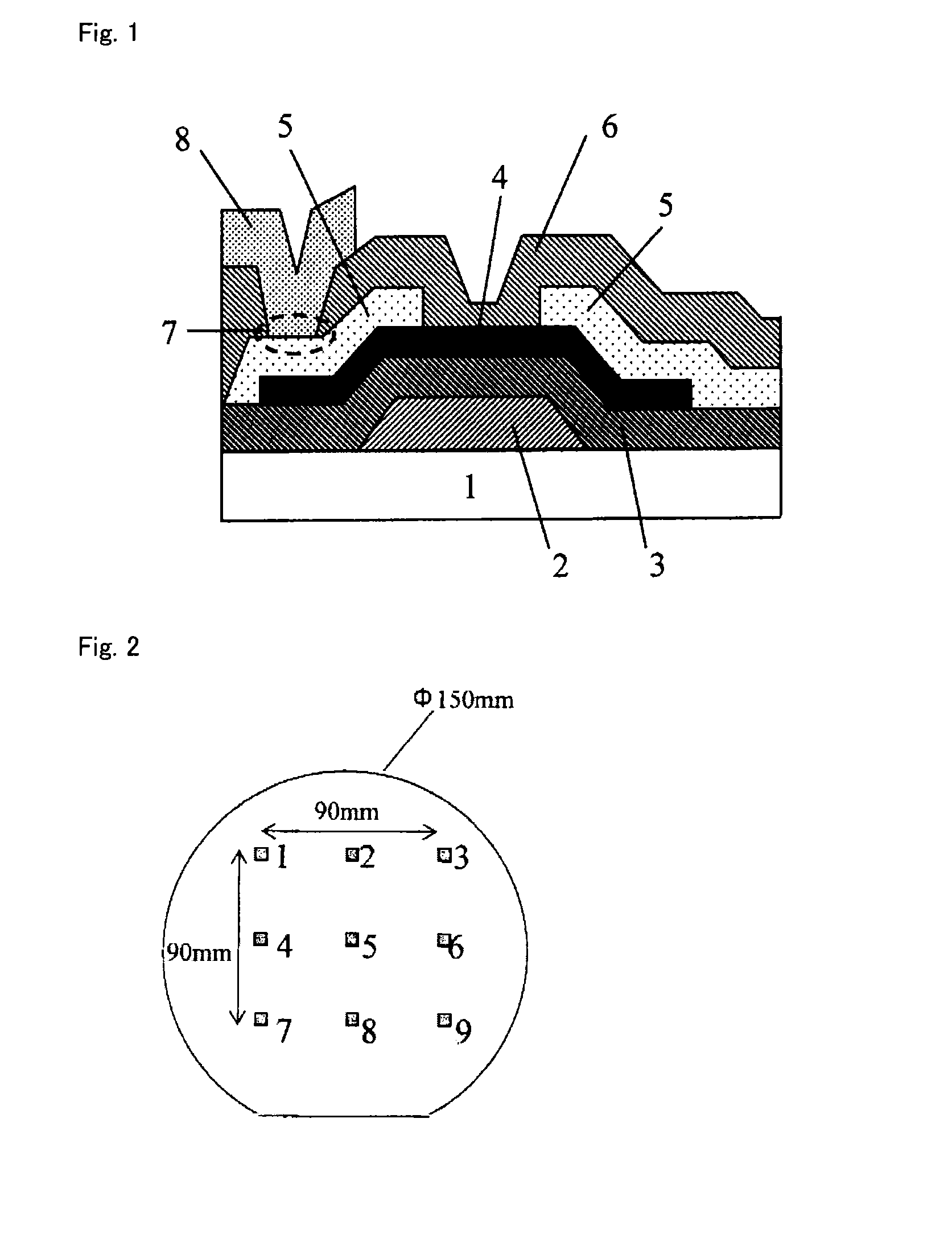
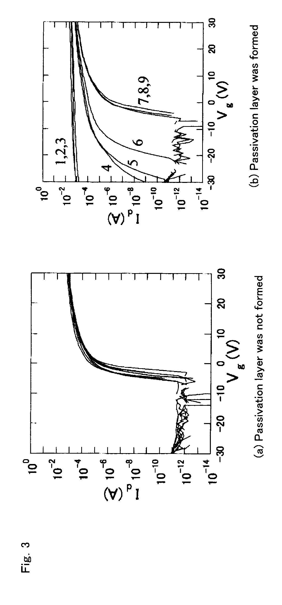
[0062]According to a method as described above, a thin-film transistor (TFT) shown in FIG. 1 was produced, and TFT characteristics before and after the formation of a passivation layer were evaluated.

[0063]First, a Ti thin film having a thickness of 100 nm as a gate electrode and a gate insulator layer of SiO2 (having a thickness of 200 nm) were successively formed on a glass substrate (“EAGLE 2000” available from Corning Incorporated, having a diameter 100 mm and a thickness of 0.7 mm). The gate electrode was formed using a pure Ti sputtering target by a DC sputtering method under the conditions: film formation temperature, room temperature; film formation power, 300 W; carrier gas, Ar; and gas pressure, 2 mTorr. Further, the gate insulator layer was formed by a plasma CVD method under the conditions: carrier gas, a mixed gas of SiH4 and N2O; film formation power, 100 W; and film formation temperature, 300° C.

[0064]Then, oxide thin films having various compositions as shown in Tabl...

example 2

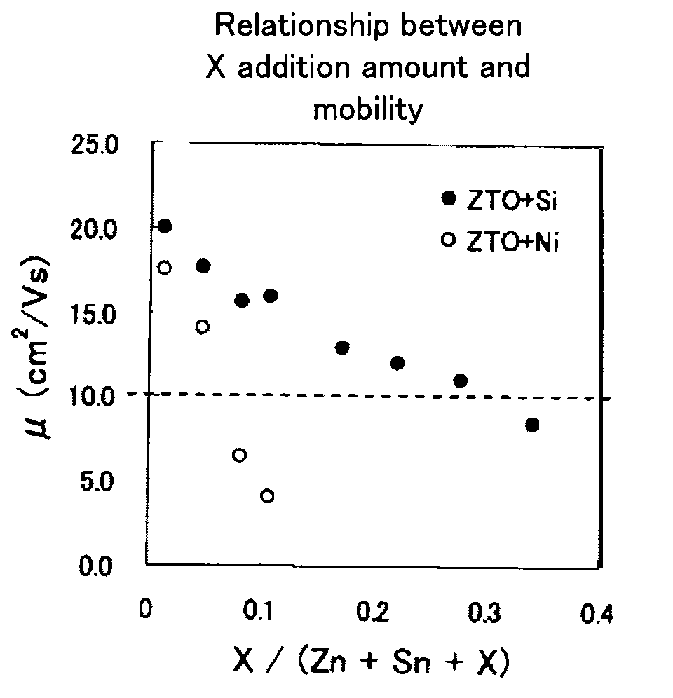
[0115]In this Example, oxide films (having a thickness of 100 nm) were measured for density, which oxide films had been obtained using the oxide with a composition corresponding to No. 4 in Table 1 (i.e., Zn—Sn-5 at % Si—O, [Zn]:[Sn]=6:4, Zn ratio=[Zn] / ([Zn]+[Sn])=0.6, Si ratio=[Si] / ([Zn]+[Sn]+[Si])=0.05) and controlling pass pressure during the sputtering film formation to 1 mTorr or 5 mTorr. Further, with respect to TFTs produced in the same manner as described above in Example 1, carrier mobility (or field-effect mobility) was calculated using the expression described below. In this Example, those in which saturated mobility thus determined was 5 cm2 / Vs or higher were considered as passing. Further, the amount of threshold voltage change (ΔVth) after the stress test (light illumination plus negative bias application) was examined. Their measurement methods are as follows:

[0116]Id=12⁢μFE⁢COX⁢WL⁢(Vgs-Vth)2[Mathematical⁢⁢Expression⁢⁢2]

where Cox is the insulator layer capacitance;

[01...


PUM

PropertyMeasurementUnit
Densityaaaaaaaaaa
Densityaaaaaaaaaa
Densityaaaaaaaaaa

Abstract

There is provided an oxide for semiconductor layers of thin-film transistors, which oxide can provide thin-film transistors with excellent switching characteristics and by which oxide favorable characteristics can stably be obtained even after the formation of passivation layers. The oxide to be used for semiconductor layers of thin-film transistors according to the present invention includes Zn, Sn, and Si.

Description

CROSS REFERENCE TO RELATED APPLICATIONS[0001]The present application is a 35 U.S.C. §371 national stage patent application of International patent application PCT / JP2011 / 067332, filed on Jul. 28, 2011, published as WO 2012 / 014999 on Feb. 2, 2012, the text of which is incorporated by reference, and claims the benefit of the filing date of Japanese application nos. JP 2010-172868, filed on Jul. 30, 2010, and JP 2011-008323, filed on Jan. 18, 2011, the text of each also being incorporated by reference.TECHNICAL FIELD[0002]The present invention relates to an oxide for semiconductor layers of thin-film transistors (TFTs) to be used in display devices such as liquid crystal displays and organic EL displays; a sputtering target for forming an oxide as described above into a film; and a thin-film transistor.BACKGROUND ART[0003]As compared with widely used amorphous silicon (a-Si), amorphous (non-crystalline) oxide semiconductors have high carrier mobility (also called as field-effect mobili...

Claims


Application Information

Patent Timeline
IPC IPC(8): H01B1/08C23C14/08H01L29/24H01L21/02H01L29/786
CPCH01B1/08C23C14/08H01L21/02554H01L21/02565H01L21/02631H01L29/24H01L29/7869
Inventor MORITA, SHINYAMIKI, AYAIWANARI, YUMIKUGIMIYA, TOSHIHIROYASUNO, SATOSHIPARK, JAE, WOOLEE, JE, HUNAHN, BYUNG, DU
Owner SAMSUNG DISPLAY CO LTD
Why Eureka
Try Eureka