Optical modulator including grapene

a technology of optical modulators and grapene, applied in optics, instruments, nanotechnology, etc., can solve the problems of high cost, stringent fabrication tolerance, and semiconductor-based electro-optical modulators

Active Publication Date: 2016-06-07
RGT UNIV OF CALIFORNIA
View PDF9 Cites 8 Cited by
  • Summary
  • Abstract
  • Description
  • Claims
  • Application Information

AI Technical Summary

Benefits of technology

[0012]Embodiments of the present invention provide an integrated optical modulator with high modulation speed, small footprint, and large optical bandwidth. Embodiments of the present invention provide a broadband, high-speed, waveguide-integrated electro-absorption modulator based on monolayer graphene. By electrically tuning the Fermi level of the graphene sheet, embodiments of the present invention can achieve over 1 GHz modulation of the guided light with a broad operation spectrum ranging from 1.35-1.6 μm under ambient conditions. Embodiments of the present invention include an active device area of merely 25 μm2.
[0013]Embodiments of the present invention provide an integration of graphene with an optical waveguide, which greatly increase the interaction length with light through the coupling between the evanescent waves and graphene. Embodiments of the present invention can open new routes to integrated photonics with a compact footprint, low voltage operation, and ultrafast modulation across a broad range of wavelengths.
[0014]By way of the graphene-based optical modulator of the present invention, having a broad optical bandwidth (1.35-1.6 μm), small device footprint (25 μm2), and high operation speed (1.2 GHz at 3 dB) under ambient conditions, essential capabilities for optical interconnects for future integrated opto-electronic systems, are provided. The flexibility of graphene sheets could also enable radically different photonic devices. For example, it can be integrated with flexible substrate and plastic waveguides. Or it can be used in novel geometries such as core-shell modulator of nano-optical cable. The recent development of large scale graphene synthesis and transfer techniques ensures its comparability with the existing integrated electronics platform.
[0015]In one embodiment of the present invention a single layer graphene optical modulator is provided. In another embodiment of the present invention a multi-layer graphene optical modulator is provided. The modulator of this embodiment uses a similar structure as a forward / reverse-biased silicon modulator in which the doped silicon is replaced by intrinsic / predoped graphene, removing the insertion loss due to the doped silicon waveguide. Both electrons and holes are injected into graphene layers to form a p-oxide-n like junction, and the optical loss from silicon can be reduced to a minimum.
[0017]Embodiments of the present invention avoid the participation of electrons / holes in silicon, and therefore its operation speed could be only limited by the carrier mobility in graphene. In addition, using two graphene layers for the active medium in embodiments of the present invention can further increase the optical absorption and modulation depth, giving advantages including smaller footprints and lower power consumptions.

Problems solved by technology

However, it has been found that the prior art semiconductor-based electro-optical modulators have disadvantages, including stringent fabrication tolerance, high cost, large device footprint, and high optical loss.
The device footprint of silicon-based modulators is on the order of millimeters, with these devices being limited by their weak electro-optical properties.
Germanium and compound semiconductors, on the other hand, face the major challenge of integration with existing silicon electronics and photonics platforms.
However, these devices suffer from intrinsic narrow-bandwidth, aside from their sophisticated optical design, stringent fabrication, and temperature tolerances.

Method used


Image

  • Optical modulator including grapene
  • Optical modulator including grapene
  • Optical modulator including grapene

Examples


example 1

Single Layer Graphene Optical Modulator

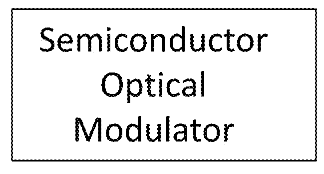
[0043]The present invention provides a waveguide-integrated graphene-based modulator that includes actively tuning the Fermi level of a monolayer graphene sheet. The gigahertz graphene modulator demonstrates a strong electro-absorption (EA) modulation of 0.1 dB / μm and operates over a broad range of wavelength from 1.35 μm to 1.6 μm under ambient conditions.

[0044]The structure of the EA modulator is schematically illustrated in FIG. 2A and FIG. 2B. A 50-nm-thick Si layer was used to connect the 250-nm-thick Si bus waveguide 210 and one of the gold electrodes. Both the silicon layer and waveguide 210 were doped with boron to reduce the sheet resistance (boron doped spin-on-glass, 850° C., 180 sec.). Seven-nm-thick Al2O3 was then uniformly deposited on the surface of waveguide 210 by atomic layer deposition (ALD) as spacer 212. A graphene sheet 214 grown by chemical vapor deposition (CVD) was then mechanically transferred onto the Si waveguide 210...

example 2

Multi-layer Graphene Optical Modulator

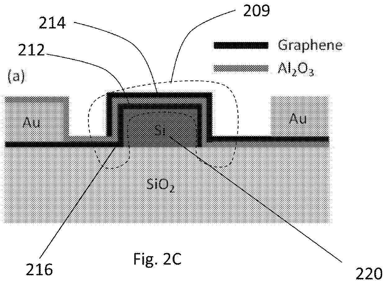
[0059]This example provides a multi-layer graphene optical modulator at high modulation depth (˜0.16 dB / μm). By using two graphene layers 214 and 216 to form a p-oxide-n like junction, embodiments of the present invention avoid the insertion loss from doped silicon and can potentially work at high frequency.

[0060]The structure of an embodiment of the present invention is schematically illustrated in FIG. 2C and FIG. 2D. In an exemplary embodiment, the fabrication of the embodiment of the present invention starts with commercial silicon-on-insulator (SOI) wafers, with a device layer thickness of 340 nm, and a buried-oxide thickness of 2 μm. A 400 nm-wide silicon waveguide 220 with both ends connected to a pair of grating couplers (period=780 nm, optimized for λ=1537 nm) was fabricated using deep reactive-ion etch (DRIE). Atomic layer deposition (ALD) technique was then employed to conformally coat a 5 nm thick Al2O3 isolation layer to prevent pot...


PUM

PropertyMeasurementUnit
carrier mobilityaaaaaaaaaa
areaaaaaaaaaaa
optical bandwidthaaaaaaaaaa

Abstract

The present invention provides for a one or more layer graphene optical modulator. In a first exemplary embodiment the optical modulator includes an optical waveguide, a nanoscale oxide spacer adjacent to a working region of the waveguide, and a monolayer graphene sheet adjacent to the spacer. In a second exemplary embodiment, the optical modulator includes at least one pair of active media, where the pair includes an oxide spacer, a first monolayer graphene sheet adjacent to a first side of the spacer, and a second monolayer graphene sheet adjacent to a second side of the spacer, and at least one optical waveguide adjacent to the pair.

Description

RELATED APPLICATIONS[0001]This application is a continuation-in-part of PCT Application No. PCT / US2012 / 034418, filed Apr. 20, 2012, which claims priority to U.S. Provisional Patent Application No. 61 / 478,467, filed Apr. 22, 2011 and to U.S. Provisional Patent Application 61 / 598,471, filed Feb. 14, 2012, all of which are herein incorporated by reference.STATEMENT OF GOVERNMENT SUPPORT[0002]This invention was made with government support under Contract No. DE-AC02-05CH11231 awarded by the U.S. Department of Energy. The government has certain rights in this invention.TECHNICAL FIELD[0003]The present invention relates to the field of optical modulators, and particularly relates to graphene based optical modulators, including both a single layer and a multi-layer graphene based modulator.BACKGROUND[0004]Optical modulators with high modulation speed, small footprint, and large optical bandwidth are needed as the enabling device for on-chip optical interconnects.[0005]Semiconductor optical...

Claims


Application Information

Patent Timeline
Patent Type & Authority Patents(United States)
IPC IPC(8): G02F1/025G02F1/015B82Y20/00
CPCG02F1/025B82Y20/00G02F2001/0156G02F2202/02G02F1/0156
Inventor LIU, MINGYIN, XIAOBOZHANG, XIANG
Owner RGT UNIV OF CALIFORNIA
Why Eureka
Try Eureka