
Germanium metal-contact-free near-IR photodetector

a metal contact-free, near-ir technology, applied in the field ofgermanium photodetectors, can solve the problems of link power budget constraints, on-chip coupling loss is usually quite high, and on-chip devices tend to be lossy as well, so as to achieve greater measurement quantum efficiency, measured quantum efficiency, and measured quantum efficiency

Active Publication Date: 2016-09-06
NOKIA SOLUTIONS & NETWORKS OY
View PDF5 Cites 19 Cited by
  • Summary
  • Abstract
  • Description
  • Claims
  • Application Information

AI Technical Summary

Benefits of technology

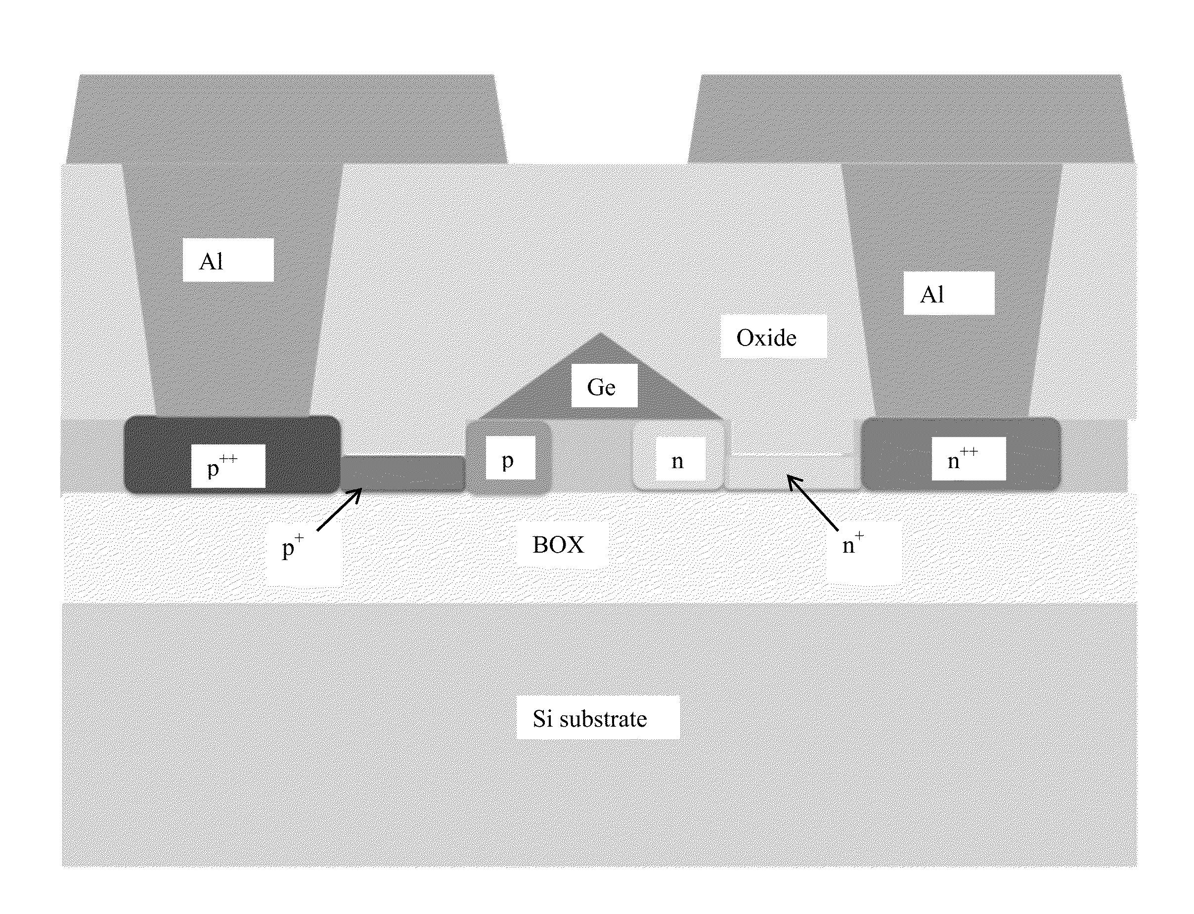
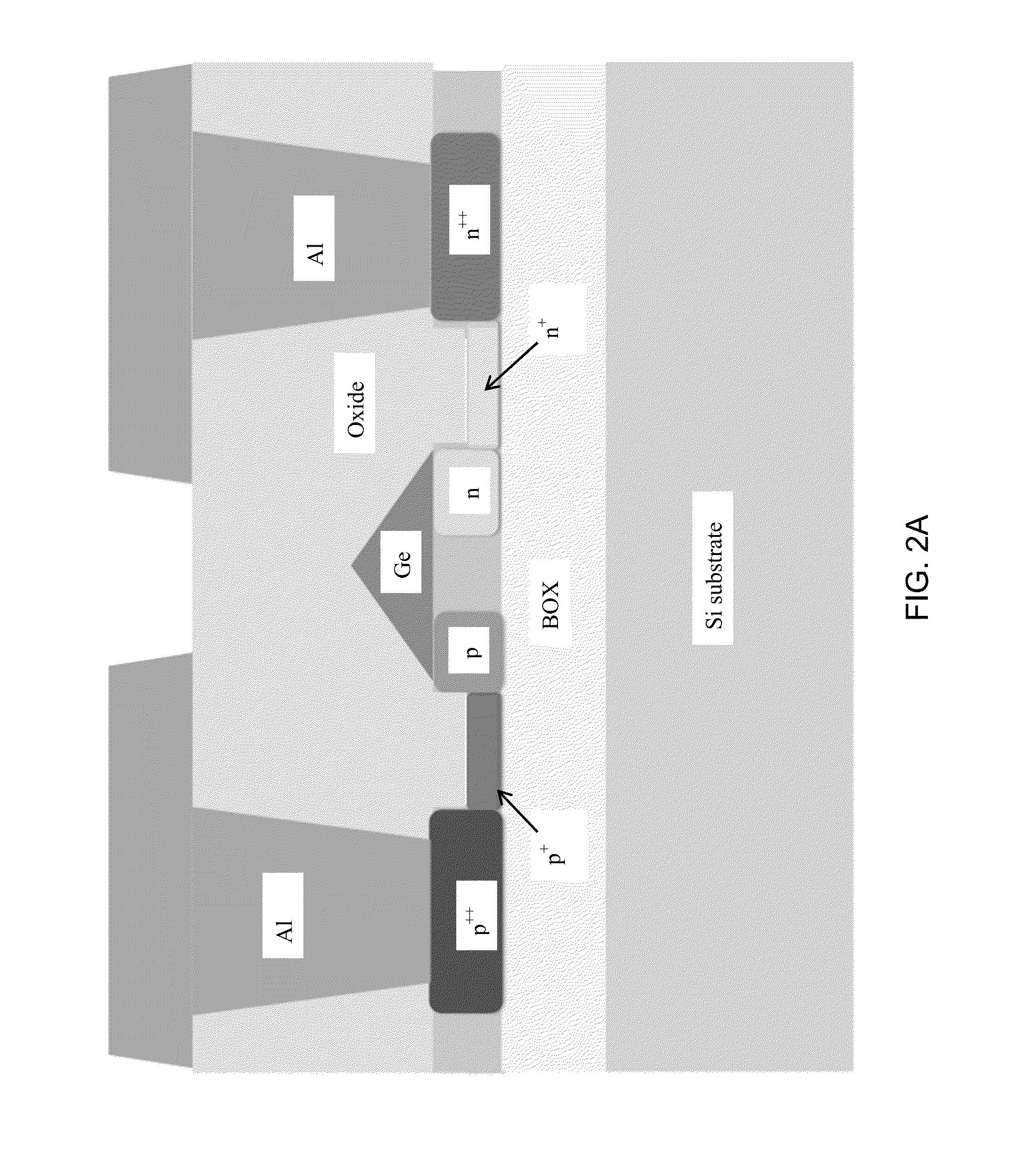
The invention is a germanium photodetector with a floating germanium body that has a triangular cross section and is oriented at an angle between 15 degrees and 75 degrees to the surface of a silicon wafer. The detector includes a first doped semiconductor contact, a second doped semiconductor contact, and an intrinsic germanium body in electrical contact with both contacts. The detector is sensitive to electromagnetic radiation in the wavelength range of 1280-1600 nm in free space. The detector can be used for detecting and measuring the intensity of electromagnetic radiation. The method of detecting electromagnetic radiation involves receiving the radiation, generating electrical signals, and displaying or recording the signals. The detector can be fabricated using a doped semiconductor wafer and metallization. The technical effects of the invention include high quantum efficiency, single optical mode operation, and conduction mode or avalanche photodiode mode operation.

Problems solved by technology

Transceivers and switch fabrics monolithically integrated with electronics have been reported.
One bottleneck that emerges during the design of silicon photonics based data links is the constraint on link power budget.
Due to the large mode mismatch of glass fibers and submicron silicon waveguides, on-and-off chip coupling loss is usually quite high.
On-chip devices tend to be lossy as well.
However, in other cases, insertion loss and device efficiency are orthogonal, for example, higher doping results in higher modulation efficiency, but leads to high insertion loss at the same time.

Method used


Image

  • Germanium metal-contact-free near-IR photodetector
  • Germanium metal-contact-free near-IR photodetector
  • Germanium metal-contact-free near-IR photodetector

Examples


Embodiment Construction

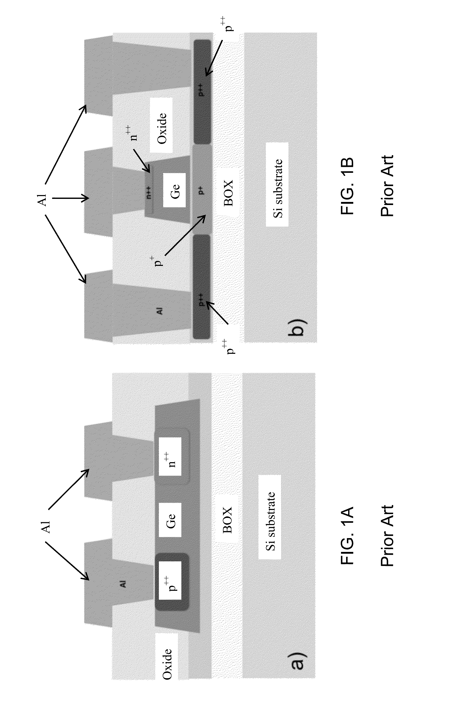
[0048]We describe a novel floating germanium photodetector that significantly simplifies Ge-on-Si detector fabrication process by eliminating the need to dope and contact germanium. The epitaxial Ge is not deliberately doped. It keeps germanium intact from damage and preserves the crystal quality after epitaxy. The device was measured to have responsivity of 1.24 A / W at 1550 nm wavelength, corresponding to 99.2% quantum efficiency. To the best of our knowledge, this is the highest responsivity reported for p-i-n germanium detectors. At −4V reverse bias, dark current is only 40 nA. The measured 3-dB bandwidth is 30 GHz and capacitance is 8 fF. The detector functions for optical radiation with free-space wavelengths from 1280-1600 nm.

[0049]The detector geometry allows the optical radiation to be is coupled predominantly into a single mode within the combined Ge / silicon detector geometry, thus maximizing the chance for absorption. It is believed that the optical mode is prevented from ...


PUM


Abstract

A Ge-on-Si photodetector constructed without doping or contacting Germanium by metal is described. Despite the simplified fabrication process, the device has responsivity of 1.24 A / W, corresponding to 99.2% quantum efficiency. Dark current is 40 nA at −4 V reverse bias. 3-dB bandwidth is 30 GHz.

Description

CROSS-REFERENCE TO RELATED APPLICATIONS[0001]This application claims priority to and the benefit of U.S. provisional patent application Ser. No. 61 / 950,816, filed Mar. 10, 2014, which application is incorporated herein by reference in its entirety.STATEMENT REGARDING FEDERALLY FUNDED RESEARCH OR DEVELOPMENT[0002]This invention was made with government support under Grants FA9550-13-1-0027 and FA9550-10-1-0439 awarded by AFOSR. The government has certain rights in the invention.FIELD OF THE INVENTION[0003]The invention relates to photodetectors in general and particularly to germanium photodetectors.BACKGROUND OF THE INVENTION[0004]Traffic on the Internet keeps growing, due in large part to the increasing demand from mobile devices, streaming media services, cloud computing, and big data analysis. Silicon photonics is promising for providing high-speed, low energy consumption and low cost next generation data communication systems. The last decade has witnessed dramatic improvement a...

Claims


Application Information

Patent Timeline
Patent Type & Authority Patents(United States)
IPC IPC(8): G01J5/20H01L31/107H01L31/0352H01L31/028H01L27/146H01L31/00H01L31/0256
CPCH01L31/0256H01L27/14638H01L27/14685H01L27/14698H01L31/028H01L31/0352H01L31/107H01L27/14649H01L31/105Y02E10/547H01L31/1808
Inventor BAEHR-JONES, THOMASZHANG, YIHOCHBERG, MICHAEL J.NOVACK, ARI
Owner NOKIA SOLUTIONS & NETWORKS OY
Learn More