Conductive through-polymer vias for capacitative structures integrated with packaged semiconductor chips

a capacitative structure and polymer via technology, applied in the direction of semiconductor/solid-state device details, printed capacitor incorporation, printed circuit non-printed electric components, etc., can solve the problems of increasing the footprint of the module and the consumption area, and achieve high capacitance density, avoid device failure, and high operating frequency

Active Publication Date: 2017-02-14
TEXAS INSTR INC
View PDF8 Cites 6 Cited by
  • Summary
  • Abstract
  • Description
  • Claims
  • Application Information

AI Technical Summary

Benefits of technology

[0009]The conductive through-polymer-vias of the invention are distinguished by the absence of a problem of mismatched coefficients of thermal expansion (which is known to plague through-silicon-vias), avoiding device failures due to delamination and temperature cycling.
[0010]The methodology is flexible and applicable to diverse devices with a single semiconductor chip, as well as to devices such as power supply systems with multiple chips. Due to the capacitors combining high capacitance density, high operating frequency, and miniscule size, the semiconductor devices may have small overall sizes in the low millimeter range; they further demonstrate stability of capacitance and frequency, and exhibit high reliability in high and low temperatures and in temperature swings.
[0011]For the preferred application to power supply systems, it is a technical advantage that the new methodology reduces electrical parasitics by placing the input capacitor in close proximity to the active circuitry. The reduced parasitic inductance allows an increase of switching frequency, which in turn allows a shrinkage of the bulky output inductor.
[0012]It is another technical advantage that the preferred process flow enables concurrent lithography through a plurality of consecutively applied polymeric compounds and a concurrent curing process of the polymers.

Problems solved by technology

This approach consumes area and increases the footprint of the module.

Method used


Image

  • Conductive through-polymer vias for capacitative structures integrated with packaged semiconductor chips
  • Conductive through-polymer vias for capacitative structures integrated with packaged semiconductor chips
  • Conductive through-polymer vias for capacitative structures integrated with packaged semiconductor chips

Examples


Embodiment Construction

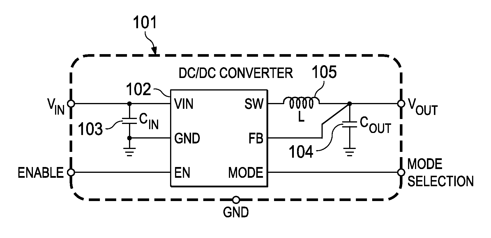
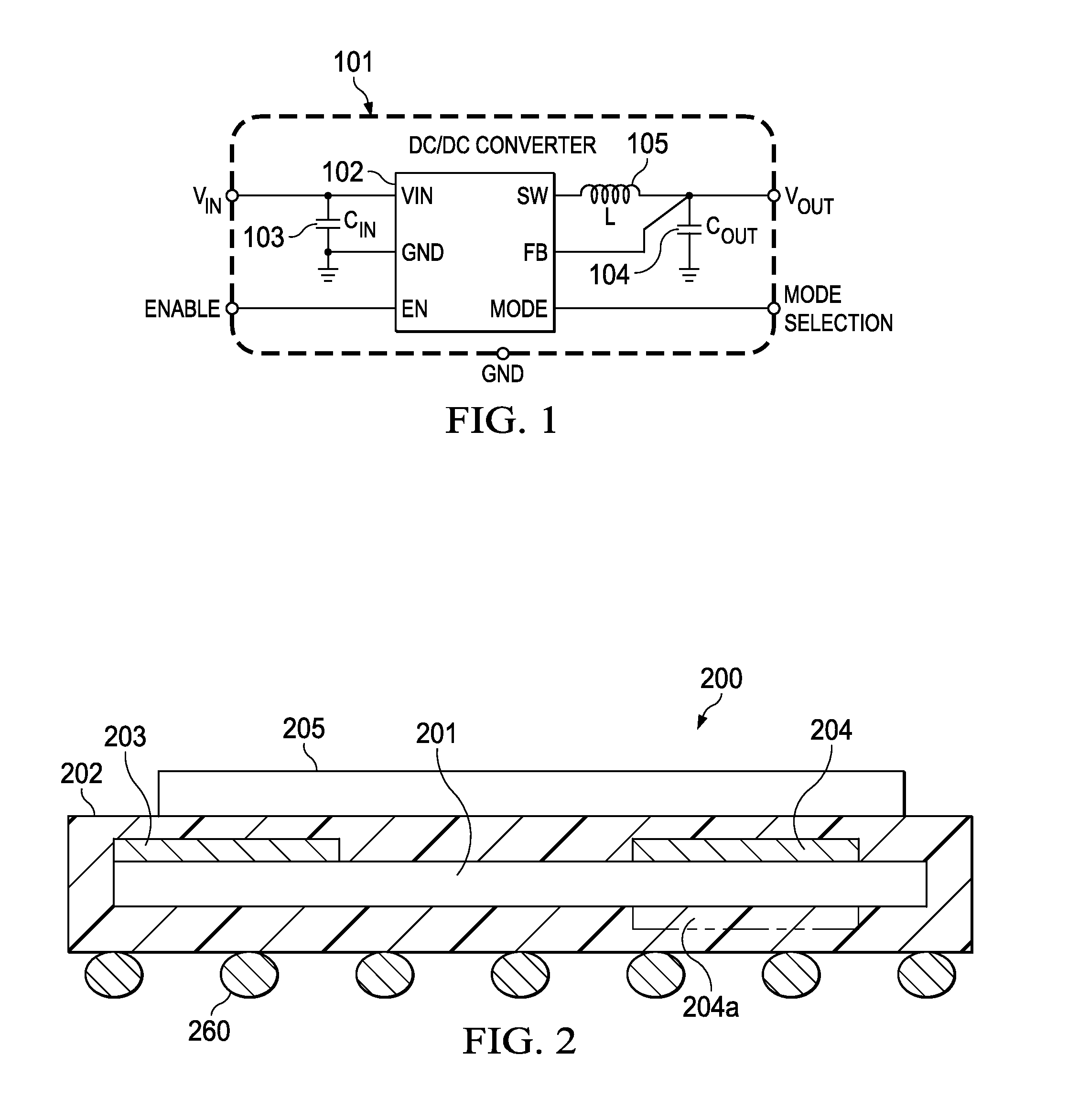
[0033]In the circuit diagram of FIG. 1, the power supply, exemplified by the dashed outline 101, includes DC / DC converter 102, input capacitor CIN (103), output capacitor COUT (104), and inductor L (105). FIG. 2 illustrates an actualization of a power supply as an exemplary silicon-in-package device 200 for board attachment with solder balls 260. Device 200 is based on an embodiment of the invention. Device 200 includes semiconductor body 201 in a package 202, input capacitor CIN (203), output capacitor COUT (204), and inductor L (205). Semiconductor body may be a single silicon chip, or an assembly of more than one chip. It should be stressed that more generally, body 201 may be an electronic body, which may include an assembly of one or more semiconductor chips, or generally may include electronic circuitry.

[0034]As the power supply of FIG. 2 shows, both capacitors are embedded with semiconductor body 201, while the inductor 205, serving as the energy storage of the power supply c...


PUM


Abstract

An electronic system comprising an electronic body (301) with terminal pads (310) and at least one capacitor embedded in the electronic body. The capacitor including an insulating and adhesive first polymeric film (302) covering the body surface except the terminal pads; a sheet (320) of high-density capacitive elements, the first capacitor terminal being a metal foil (321) attached to film (302), the second terminal a conductive polymeric compound (324), and the insulator a dielectric skin (323). Sheet (320) has sets of via holes: the first set holes reaching metal foil 321), the second set holes reaching the terminals (310), and the third set holes reaching the conductive polymeric compound (324). An insulating second polymeric film (303) lining the sidewalls of the holes and planarizing the sheet surface; and metal (432) filling the via holes between the polymeric sidewalls and forming conductive traces and attachment pads on the system surface.

Description

FIELD[0001]Embodiments of the invention are related in general to the field of semiconductor devices and processes, and more specifically to the structure and fabrication method of electronic systems encapsulated in a package with embedded nanometer-sized three-dimensional capacitors.DESCRIPTION OF RELATED ART[0002]Among the popular families of power supply circuits are the power switching devices for converting one DC voltage to another DC voltage, the DC / DC converters. Particularly suitable for the emerging power delivery requirements are the Power Blocks with two power MOS field effect transistors (FETs) connected in series and coupled together by a common switch node; such assembly is also called a half bridge. When a regulating driver and controller is added, the assembly is referred to as Power Stage or, more commonly, as Synchronous Buck Converter or Voltage Regulator. In the synchronous Buck converter, the control FET chip, also called the high-side switch, is connected betw...

Claims


Application Information

Patent Timeline
Patent Type & Authority Patents(United States)
IPC IPC(8): H05K1/18
CPCH05K1/185H05K1/181H05K1/113H05K1/162H05K2201/0187H05K2201/0215H05K2201/10734H01L21/288H01L21/31051H01L21/76805H01L21/76831H01L21/76874H01L21/76877H01L21/78H01L23/5223H01L23/5226H01L23/528H01L24/14H01L28/60H01L2924/19011H01L2924/19041H01L2924/19042H01L2924/19104
Inventor ROMIG, MATTHEW D.STEPNIAK, FRANKGANDHI, SAUMYA
Owner TEXAS INSTR INC
Why Eureka
Try Eureka