

Sputtering target and method for producing same
a technology of sputtering target and target, which is applied in the direction of sustainable manufacturing/processing, final product manufacturing, vacuum evaporation coating, etc., can solve the problem of slow speed of vapor deposition film-forming method for forming film, and achieve the effect of improving power generation efficiency and high power generation efficiency
- Summary
- Abstract
- Description
- Claims
- Application Information
AI Technical Summary
Benefits of technology
Problems solved by technology
Method used
Image

Examples
examples
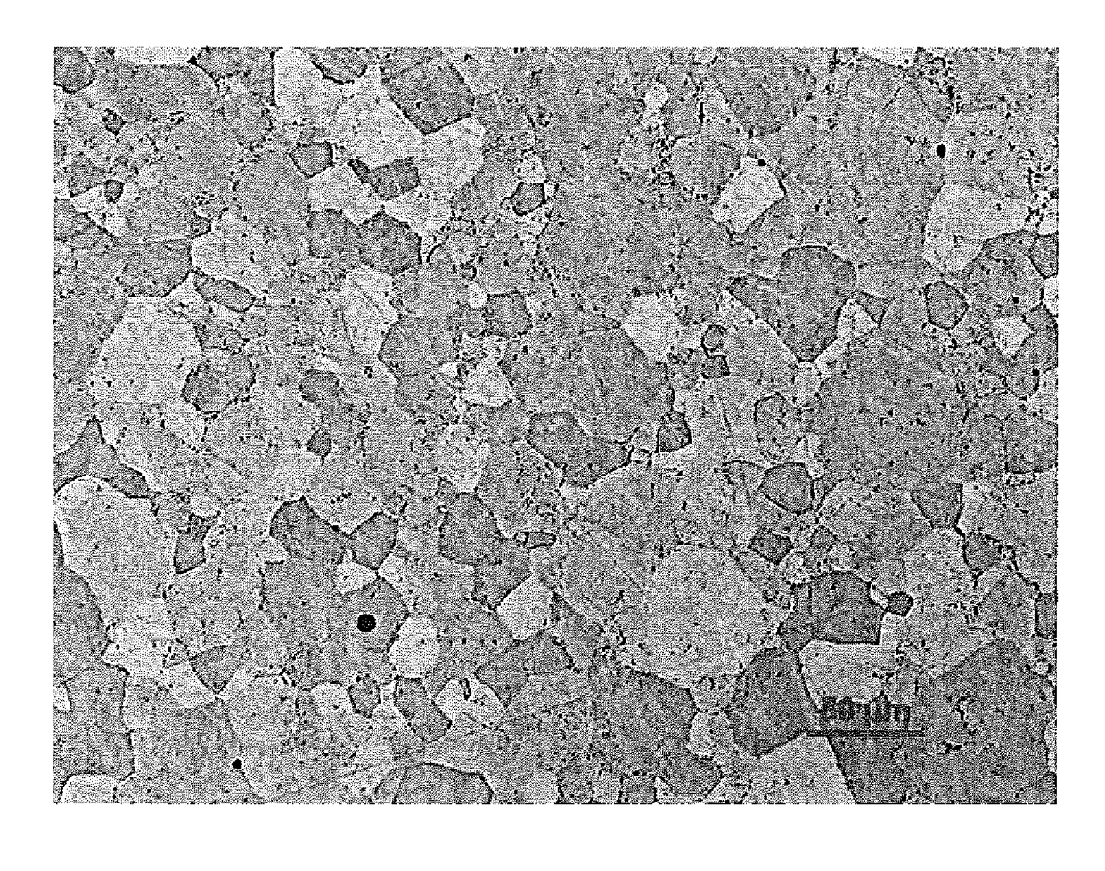
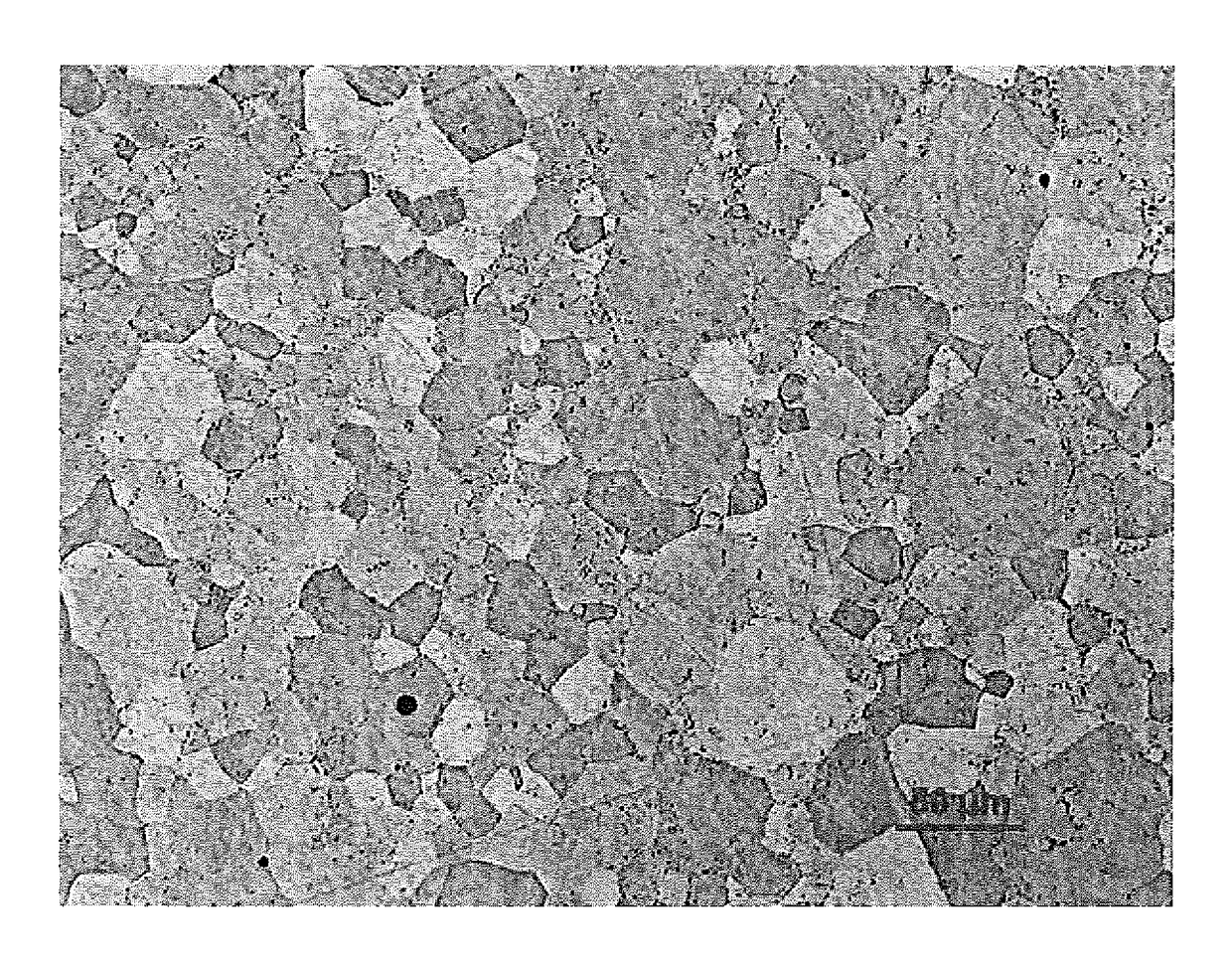
[0082]Firstly, a Cu—Ga alloy powder and a Cu powder (purity 4N) having the component composition and the particle diameter shown in Table 1 were blended with a NaF compound powder, a Na2S compound powder, or a Na2Se compound powder each having a purity of 3N and a primary mean particle diameter of 0.5 μm so as to achieve the amount thereof as shown in Table 1 to thereby produce a starting material powder in each of Examples 1 to 35. Each of these starting material powder was firstly dried in a vacuum drier in a vacuum environment of 10−1 Pa at a temperature of 120° C. for 10 hours, and then was placed in a polyethylene pot having a volume of 10 L. Then, a zirconia ball having a diameter of 5 mm dried at a temperature of 120° C. for 10 hours was further added in the pot, and the resulting mixture was mixed in a ball mill for a specified time. Mixing was performed in a nitrogen atmosphere.
[0083]The obtained mixed powder was sintered under the condition as specified in Table 2. In the ...
PUM
| Property | Measurement | Unit |
|---|---|---|
| particle diameter | aaaaa | aaaaa |
| crystal particle size | aaaaa | aaaaa |
| temperature | aaaaa | aaaaa |
Abstract
Description
Claims
Application Information