Solar cells with perovskite-based light sensitization layers
a technology of light sensitization layer and solar cell, which is applied in the direction of electrolytic capacitor manufacturing, final product manufacturing, sustainable manufacturing/processing, etc., can solve the problems of high cost of conventional photovoltaic, and achieve the effects of less toxic, less environmental pollution, and greater long-term stability
- Summary
- Abstract
- Description
- Claims
- Application Information
AI Technical Summary
Benefits of technology
Problems solved by technology
Method used
Image
Examples
example 4
Making a Metal Oxide Electron Transporting Layer
[0104]The TiO2 layer was coated on a conductive (FTO) substrate using an electrospray method After electrospraying process, the as-prepared TiO2 sphere coated electrode was heated to 130° C. from room temperature in 30 min.
Example 5—Method of Making a Solar Cell with an A2MX6 Perovskite
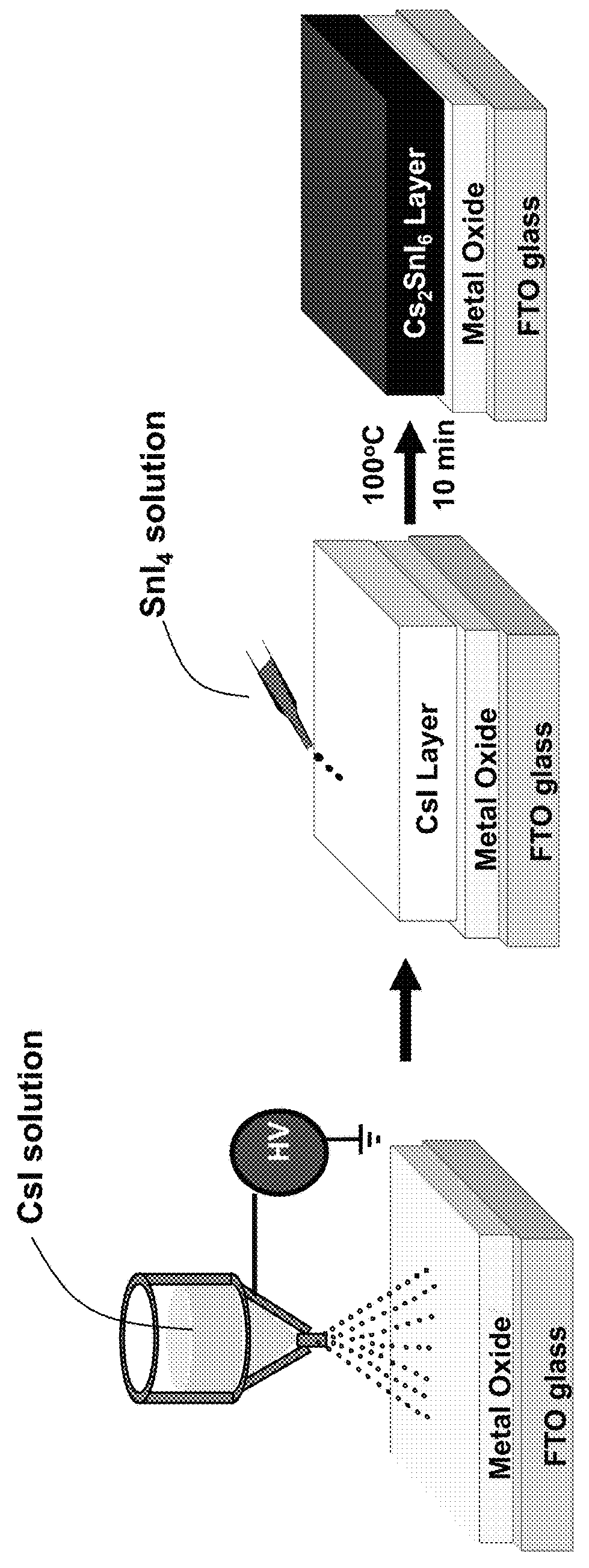
[0105]This method is illustrated in FIG. 1. Sequential deposition of Cs2SnI6 To coat different thickness of Cs2SnX6 layers, a novel two-step coating process (Electrospraying technique) has been developed in our laboratory. At the first step, a CsI solution was prepared dissolving 2 g of CsI powder (Aldrich, 99.9%) in 400 ml of the mixture solvent of deionized water and isopropanol (deionized water:isopropanol=0.1:1 v / v). After sonication for 1 hour, the solutions were loaded into a plastic syringe equipped with a 27-gauge stainless steel needle. The spinning rate was controlled by a syringe pump (KD Scientific Model 220) at 35˜50 μL / min. The electric fie...
example 9
Making a Solar Cell with a Spin-Coated Electron Transporting Layer
[0112]A solar cell device was made consisting of the following layer structure: conductive substrate (electrode) / metal oxide (thin layer by spin-coating method) / perovskite sensitizer / LPAH carbon (by electrospraying) / LPAH coated conductive substrate. (“LPAH” is large-effective-surface-area poly aromatic hydrocarbon.)
[0113]The layers of the device were made as follows. For the metal oxide (thin layer by spin-coating method), a solution of 0.2M titanium bis(ethyl acetoacetate) diisopropoxide (C18H34O8Ti, Adrich, 99.9%) in 1-butanol (Adrich, 99.8%) was prepared for compact TiO2 blocking layer. A drop of a blocking layer solution was set on the center of a conducting substrate and flattened using a spin-coating method at 2000 rpm for 60 sec. These films were sintered at 450° C. for 30 min.
[0114]For the LPAH carbon (by electrospraying), the LPAH layer was made by a hydrogen arc and the carbon solutions were prepared by disp...
example 10
Making a Solar Cell with a Mesoporous Electron Transporting Layer
[0118]A solar cell device was made consisting of the following layer structure: conductive substrate (electrode) / metal oxide (mesoporous TiO2 by electrospray method) / perovskite sensitizer (by electrospraying) / metal oxide and LPAH coated conductive substrate).
[0119]In a typical dye-sensitized solar cell (DSSC), the titanium oxide (TiO2) layer is made porous to have an increased surface area. Such a porous TiO2 layer is prepared by dispersing in water or organic solvent about 20 nm-sized anatase crystalline TiO2 nanoparticle produced by hydrothermal synthesis of titanium alkoxide, adding an organic polymer or oligomer binder to produce a paste, and coating the paste on a transparent conductive substrate from blade or screen printing coating, which evaporate or burn off when the TiO2 film is sintered at about 450˜500° C. However, the conventional methods using an organic binder have a problem in that the short-circuit cur...
PUM
 Abstract
Description
Claims
Application Information


