Method of preparing solar cell front contacts

a solar cell and front contact technology, applied in the field of preparing can solve the problems of high power dissipation, low efficiency, and low efficiency of solar cell front contacts, and achieve the effects of reducing carrier recombination losses, good barrier, and high sheet resistan

Inactive Publication Date: 2002-01-15
INTERUNIVERSITAIR MICRO ELECTRONICS CENT (IMEC VZW)
View PDF9 Cites 160 Cited by
  • Summary
  • Abstract
  • Description
  • Claims
  • Application Information

AI Technical Summary

Benefits of technology

2. Separation of the collector lines from the direct contact with silicon substrate reduces carrier recombination losses existing at the metal contact-silicon interface. Selection of material used for the ARC coating and of the deposition technique are crucial for achieving a separation. Most top contact silver pastes penetrate through an ARC layer of titanium dioxide deposited by Atmospheric Pressure Chemical Vapor Deposition (APCVD). In the case of using a silicon nitride AR layer d

Problems solved by technology

This causes a relatively high shading of the front solar cell surface.
However, the heavy emitter doping induces a poor response of the solar cell to short wavelength light.
This gives rise to increased line resistance causing high power dissipation, particularly in the main collector lines.
The fact that the fingers are ultra-thin can result in the interruption of such fingers.
Another main disadvantage of the ultra-thin screens is their higher cost and lower durability and/or reliability.
This implies a complicated design and a very high screen cost.
This is in conflict with most of the commercially available silver pastes for solar cell front contact metallization.
Silver powder has a tendency to create agglomerates of particles in the paste.
In addition, a flake-shaped silver powder, usually used in the paste formulation for a solar metallization, increases the tendencies to create agglomerates of particles in the paste.
Although commercia

Method used


Image

  • Method of preparing solar cell front contacts
  • Method of preparing solar cell front contacts
  • Method of preparing solar cell front contacts

Examples


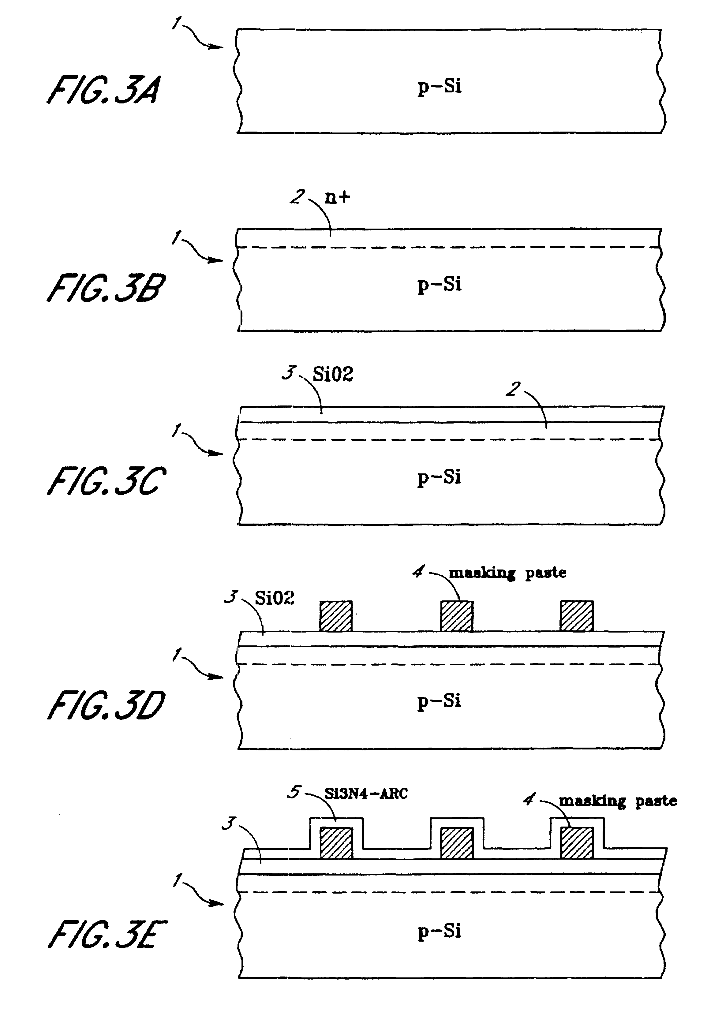
Embodiment Construction

I. Preparation of Screens

1. A standard fabric screen is stretched and glued to a frame adequate to the screen printer used. Typical parameters are metal screen of 80 UT, orientation of wires to the frame at an angle of 90.degree., and tension of the screen 30N.

2. An emulsion typical for screen patterning is deposited over the screen and dried.

3. A solid metal foil with thickness of 40-60 .mu.m is bonded at its peripheries to the standard fabric screen stretched to the frame. The meshes of the fabric screen are cut away from the middle region of the foil where the pattern will be formed.

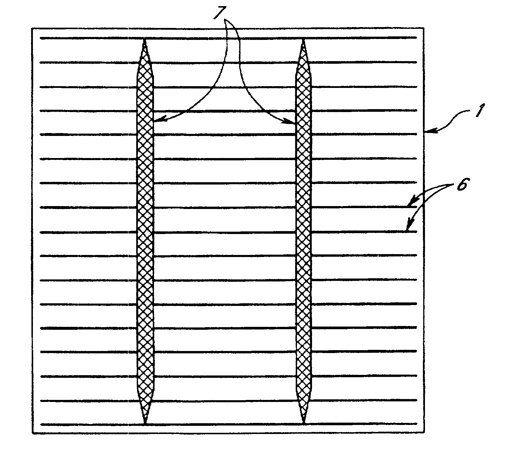
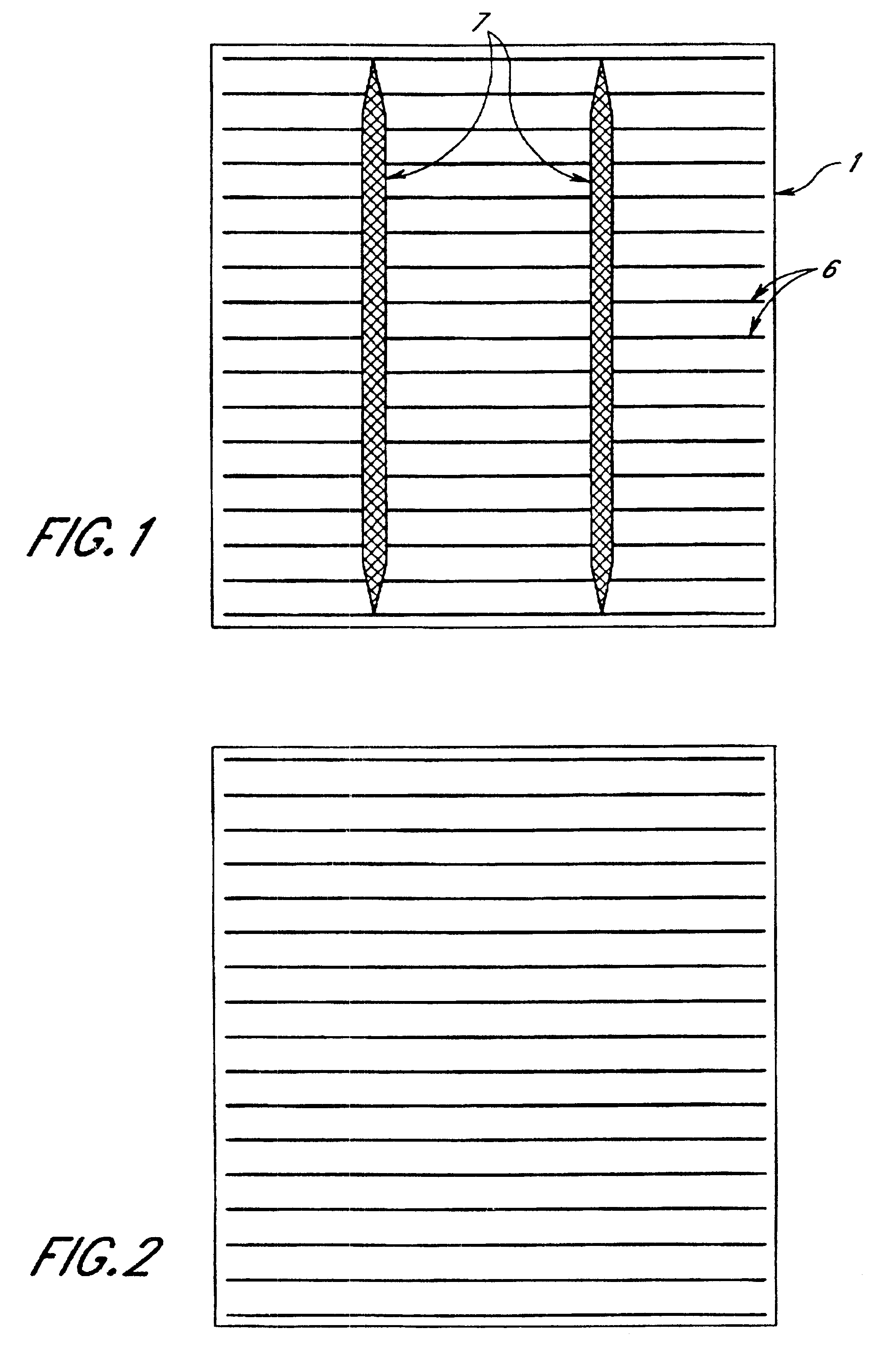
4. A set of parallel lines reflecting the finger pattern of solar cell contacts is cut by a laser beam. An electron or iron beam can also be used for the cutting process. The width of the cut lines is regulated by the beam diameter, the power, and the cutting speed. A typical contact flager screen consists of lines with width of 40-50 .mu.m and a distance between them of 1.2-1.5 mm cut in a stainless ...


PUM


Abstract

Method of preparing on a solar cell the top contact pattern which consists of a set of parallel narrow finger lines and wide collector lines deposited essentially at right angles to the finger lines on the semiconductor substrate, characterized in that it comprises at least the following steps:(a) screen printing and drying the set of contact finger lines;(b) printing and drying the wide collector lines on the top of the set of finger lines in a subsequent step;(c) firing both finger lines and collector lines in a single final step in order to form an ohmic contact between the finger lines and the semiconductor substrate and between the finger lines and the wide collector lines.

Description

OBJECT OF THE INVENTIONThe present invention is related to a method of preparing contacts on the surface of semiconductor substrates. The present invention is also related to products obtained by this method and more particularly to a solar cell.STATE OF THE ARTConventional screen printing is currently used in a mass scale production of solar cells. Typically, the top contact pattern of a solar cell consists of a set of parallel narrow finger lines and wide collector lines deposited essentially at a right angle to the finger lines on the semiconductor substrate or wafer.Such front contact formation of crystalline solar cells is performed with standard screen printing techniques. It has advantages in terms of production simplicity, automation, and low production cost.Low series resistance and low metal coverage (low front surface shadowing) are basic requirements for the front surface metallization.According to the document Hybrid Circuit No. 30, January 1993, "Thick-film Fine-line F...

Claims


Application Information

Patent Timeline
IPC IPC(8): H01L31/0224H01L31/04
CPCH01L31/022425Y02E10/50H01L31/18
Inventor SZLUFCIK, JOZEFNIJS, JOHANFICK, ROLAND JOZEF
Owner INTERUNIVERSITAIR MICRO ELECTRONICS CENT (IMEC VZW)
Why Eureka
Try Eureka