

Catadioptric projection systems
- Summary
- Abstract
- Description
- Claims
- Application Information
AI Technical Summary
Benefits of technology
Problems solved by technology
Method used
Image

Examples
Embodiment Construction
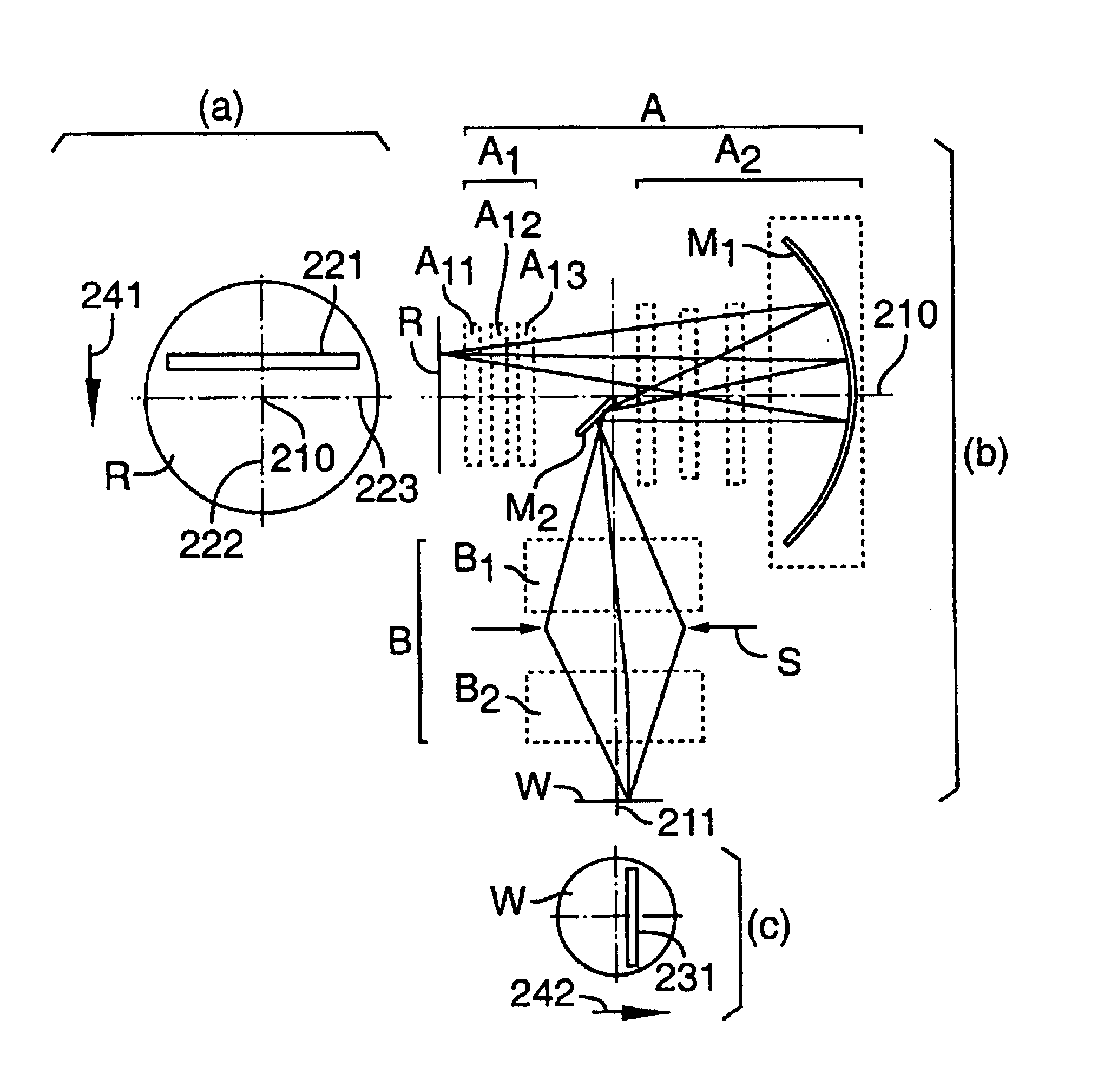
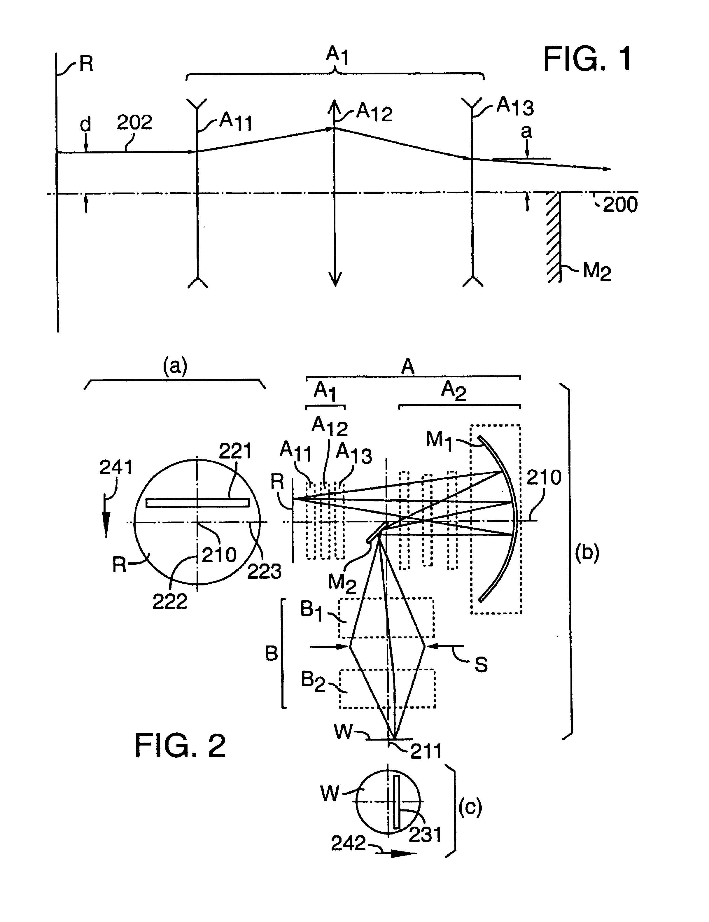
[0035]For purposes of describing the invention, a “lens element” is a single lens (i.e., a single piece of “glass”); a lens “group” or “subgroup” comprises one or more lens elements. A positive lens, lens group, or subgroup has a positive focal length; a negative lens, lens group, or subgroup has a negative focal length. An “optical axis” is a straight line through centers of curvature of surfaces of optical elements. As will be apparent, an optical system can have more than one optical axis. Distances from an off-axis point to an optical axis are measured along a line through the point and perpendicular to the optical axis.
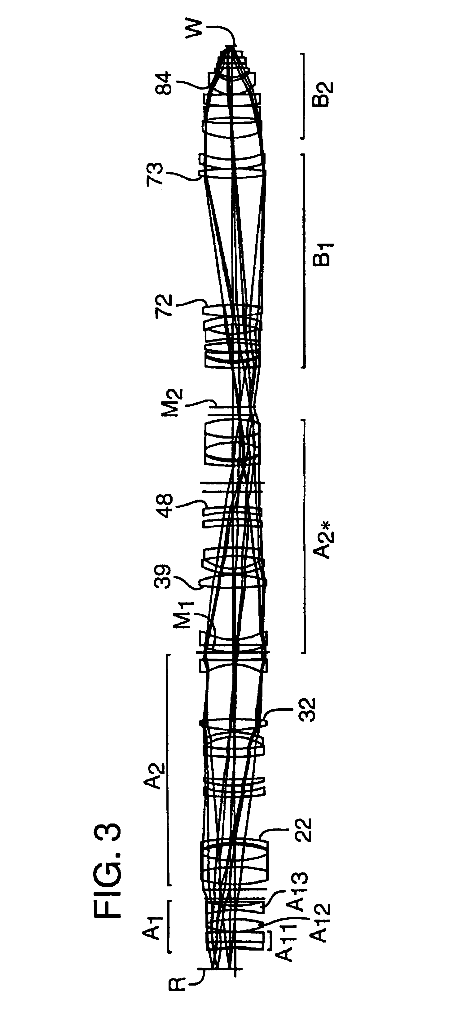
[0036]In order to describe the invention, a representation of a prior-art optical system is first described with reference to FIG. 7. A ray 102 from a location on a reticle R a distance d from an optical axis 100 is incident on a lens group A1. The lens group A1 comprises, in order from the reticle R and along the optical axis 100, a positive subgroup A12 and a n...
PUM
 Abstract
Description
Claims
Application Information