Silicon-on-insulator chip having an isolation barrier for reliability

a technology of isolation barrier and silicon on the silicon-on-insulator chip, which is applied in the field of silicon-on-insulator chip having an isolation barrier, can solve the problems of reducing the overall manufacturing yield compromising the reliability and performance of the integrated circuit, and losing manufacturing yield, so as to reduce the processing steps, reduce the exposure to reactive ion etching, and reduce the effect of charging

Inactive Publication Date: 2008-05-27
GLOBALFOUNDRIES INC
View PDF21 Cites 5 Cited by
  • Summary
  • Abstract
  • Description
  • Claims
  • Application Information

AI Technical Summary

Benefits of technology

[0014]To also overcome the shortcomings of conventional processes of manufacturing SOI chips, a new process of manufacture is provided. An object of the present invention is to reduce processing steps. A related object is to ma

Problems solved by technology

During the packaging of a semiconductor chip, impurities from the packaging environment can enter the chip, diffuse into silicon junctions, and compromise the reliability and performance of the integrated circuit.
Contamination at this particular juncture of the manufacturing process can result in loss of manufacturing yield.
The process of exposing the edges of SOI chips bef

Method used


Image

  • Silicon-on-insulator chip having an isolation barrier for reliability
  • Silicon-on-insulator chip having an isolation barrier for reliability
  • Silicon-on-insulator chip having an isolation barrier for reliability

Examples


first embodiment

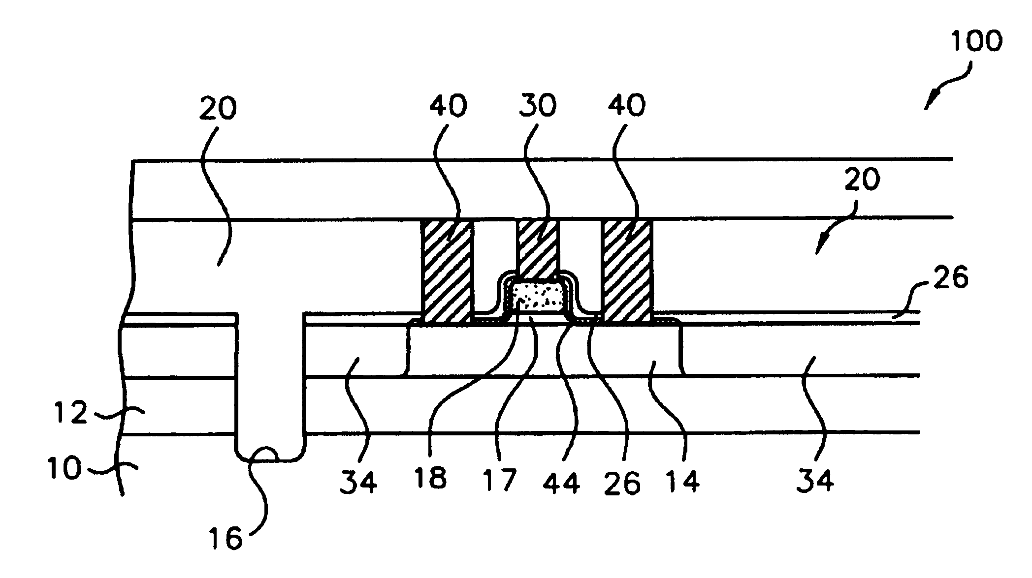
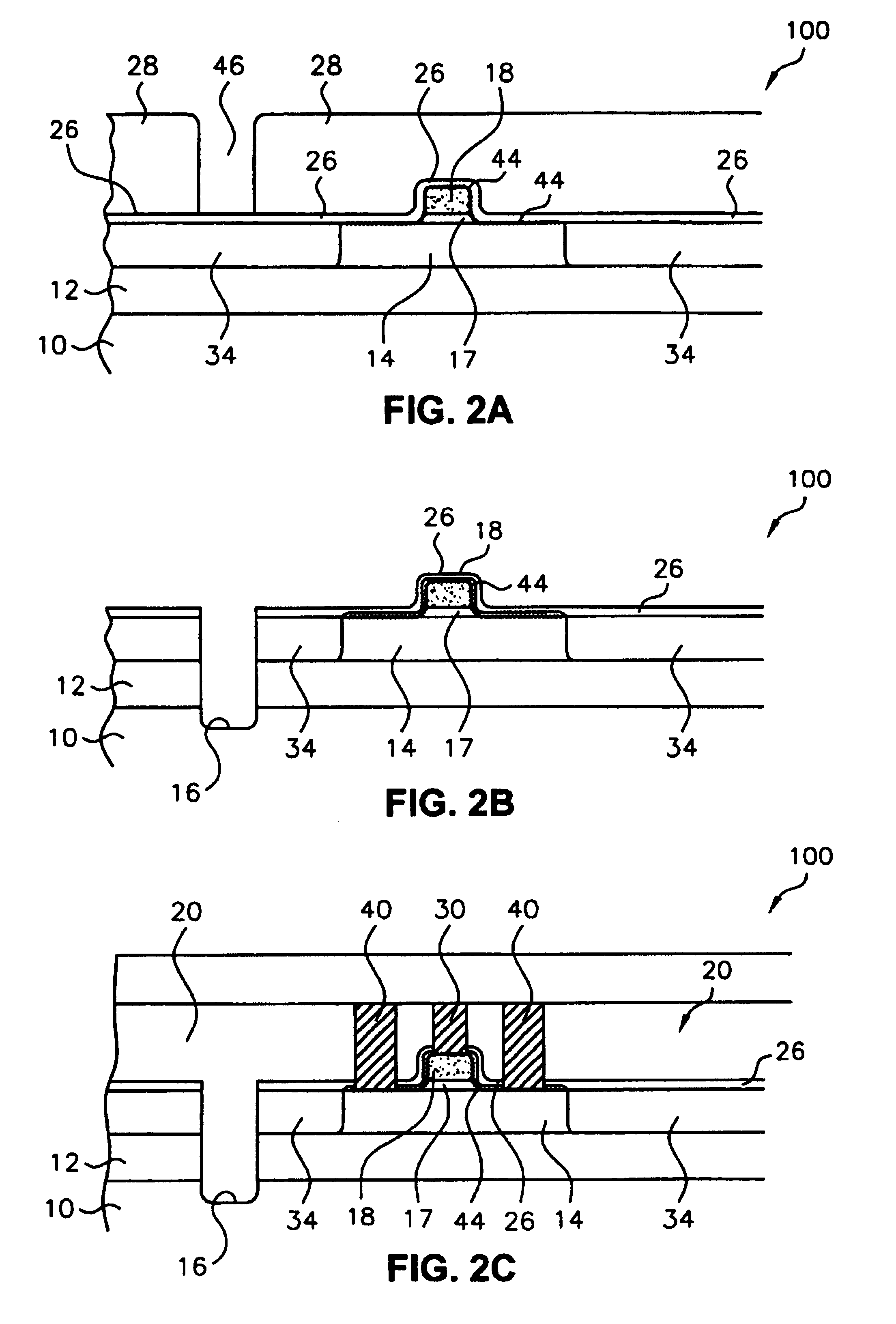
[0038]the process of manufacturing SOI chip 100 having a groove 16 as an integrated diffusion barrier includes the following steps (illustrated in FIG. 2D). First, a device having substrate 10, buried oxide layer 12, silicon layer 14 with at least one trench 34, gate 18, and silicide layer 44 is provided (Step 500). Passivation layer 26 is deposited (Step 510), resist is applied (Step 520), groove 16 is etched (Step 530), resist 28 is removed (Step 540), barrier material 20 is deposited (Step 550), barrier material 20 is polished (Step 560), metal contact lithography is performed (Step 570), and a final CMP is done (Step 580). A single photolithography mask or resist 28 is deposited (Step 520). A single reactive ion etching step is applied (Step 530). Finally, the resist 28 is stripped (Step 540).

[0039]The first embodiment of the process of manufacturing SOI chip 100 having a groove 16 as an integrated diffusion barrier requires only three extra steps over a conventional SOI chip 1 ...

second embodiment

[0042]Thus, the process of manufacturing SOI chip 101 having a groove 16 as an integrated diffusion barrier includes the following steps. First, a device having a substrate 10, buried oxide layer 12, silicon layer 14 with at least one trench 34, gate 18, and silicide layer 44 is provided (Step 500). Resist is applied (Step 520), groove 16 is etched (Step 530), and resist 28 is removed (Step 540). Then passivation layer 26 is deposited (Step 510). Subsequently, barrier material 20 is deposited (Step 550), barrier material 20 is polished (Step 560), metal contact lithography is performed (Step 570), and a final CMP is done (Step 580).

third embodiment

[0043]the SOI chip 102 of the present invention is illustrated in FIG. 4. SOI chip 102 shown in FIG. 4 is similar to SOI chip 101 of FIG. 3 in that passivation layer 24 is deposited in groove 16, and passivation layer 26 is deposited over silicon layer 14 (including trench 34) and gate 18, after groove 16 is formed in the SOI chip. Passivation layer 24 may be a dielectric such as silicon nitride or a composite of silicon dioxide and silicon nitride. Unlike the process used to manufacture SOI chip 101 of FIG. 3, however, an anisotropic etch is then applied to groove 16 of SOI chip 102. The anisotropic etch removes a portion of passivation layer 24 extending along the bottom of groove 16. Consequently, passivation layer 24 extends into groove 16 only along the side walls of groove 16 and the bottom of groove 16 is open to silicon substrate 10. Groove 16 retains the dielectric and passivation properties, however, on its side walls.

[0044]Fill material 50 is then deposited in groove 16, ...


PUM


Abstract

An SOI chip having an isolation barrier. The SOI chip includes a substrate, an oxide layer deposited on the substrate, and a silicon layer deposited on the oxide layer. A gate is deposited above the silicon layer. A first metal contact is deposited above the gate to form an electrical contact with the gate. Second and third metal contacts are deposited to form electrical contacts with the silicon layer. The isolation barrier extends through the silicon layer and the oxide layer, and partially into the substrate, to block impurities in the oxide layer outside the isolation barrier from diffusing into the oxide layer inside the isolation barrier. The isolation barrier surrounds the gate, the first metal contact, the second metal contact, and the third metal contact—which define an active chip area inside the isolation barrier. A method of manufacturing the SOI chip is also disclosed.

Description

CROSS-REFERENCE TO RELATED APPLICATIONS[0001]This applicationis a Reissue Application of U.S. Pat. No. 6,492,684, issued Dec. 10, 2002, which is a continuation-in-part of U.S. patent application Ser. No. 09 / 859,146, filed on May 16, 2001 <?delete-start id="DEL-S-00002" date="20080527" ?>(pending)<?delete-end id="DEL-S-00002" ?> <?insert-start id="INS-S-00002" date="20080527" ?>now U.S. Pat. No. 6,563,173<?insert-end id="INS-S-00002" ?>, which is a continuation of U.S. patent application Ser. No. 09 / 148,918, filed on Sep. 4, 1998 (allowed), U.S. Pat. No. 6,281,095 which is a divisional of U.S. patent application Ser. No. 09 / 009,445; filed on Jan. 20, 1998, now U.S. Pat. No. 6,133,610.FIELD OF THE INVENTION[0002]The present invention relates generally to a silicon-on-insulator (SOI) chip and, more particularly, to an SOI chip having an isolation barrier to prevent the diffusion of impurities into active regions of the chip.BACKGROUND[0003]As the scale of int...

Claims


Application Information

Patent Timeline
IPC IPC(8): H01L21/336H01L21/74H01L21/762H01L27/12H01L29/786
CPCH01L21/743H01L21/76264H01L21/76283H01L27/1203H01L29/66772H01L29/78636H01L29/78648
Inventor BOLAM, RONALD J.KULKAMI, SUBHASH B.SCHEPIS, DOMINIC J.
Owner GLOBALFOUNDRIES INC
Why Eureka
Try Eureka