Method for improving thick film GaN quality using uniform nano particle dot array mask

A nanoparticle and lattice technology, applied in the field of GaN material preparation, achieves uniform distribution, reduced dislocation density, and uniform dislocation density distribution

Inactive Publication Date: 2009-10-07
DAHOM FUJIAN ILLUMINATION TECH
View PDF2 Cites 0 Cited by
  • Summary
  • Abstract
  • Description
  • Claims
  • Application Information

AI Technical Summary

Problems solved by technology

So far, rare reports

Method used


Image

  • Method for improving thick film GaN quality using uniform nano particle dot array mask
  • Method for improving thick film GaN quality using uniform nano particle dot array mask

Examples


Embodiment 1

[0019] Embodiment 1. Preparation of thick-film GaN material for HVPE.

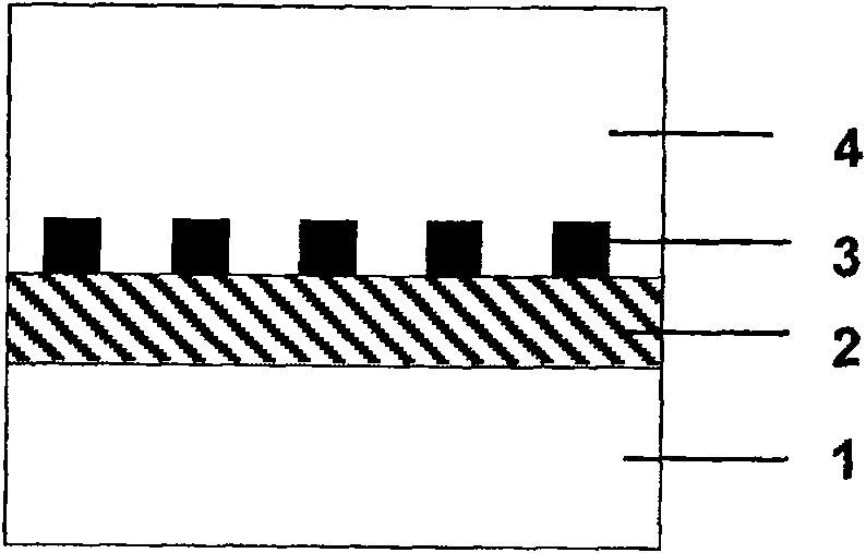
[0020] Such as figure 1 As shown, using the MOCVD method in Al 2 o 3 A GaN film of about 3 microns was grown on the substrate (0001), and this film was used as a HVPE template, and then at a temperature of 200°C, a 300nm-thick metal Al thin layer was deposited on the surface of the template by electron beam evaporation, and then the tape The template with Al layer is put into oxalic acid solution (0.3mol / L), and anodized at room temperature with a voltage of 40 volts for about 15 minutes, then the metal Al is electrochemically corroded into porous AAO with regular distribution, and then the template is placed in Soak in phosphoric acid solution (5wt%) at 30°C for 40 minutes, the purpose is to expand the pore size and remove the part of the aluminum oxide at the bottom of the small hole that is in contact with the lower layer of GaN. After cleaning, deposit 5nm thick SiO in the nanopore 2 , and finally s...

Embodiment 2

[0022] Use SiC, Si or GaAs as the substrate, and the dielectric layer implanted in the anodized aluminum hole is SiO or Si x N y, and the process steps for preparing thick film GaN are the same as those in Embodiment 1.


PUM

PropertyMeasurementUnit
thicknessaaaaaaaaaa
thicknessaaaaaaaaaa
thicknessaaaaaaaaaa

Abstract

The invention relates to a method for improving the quality of thick-film GaN by using a uniform nanoparticle lattice, which is characterized in that the nanoscale SiO2, SiO or SixNy lattice is used as a GaN epitaxial mask. Before the hydride vapor phase epitaxy, a layer of metal Al is evaporated on the GaN template by electron beam, and then the porous anodic aluminum oxide (AAO) is formed by electrochemical method, and then the lattice structure medium is injected into the hole, and then the AAO is removed. , the lattice structure of uniformly distributed SiO2 nanoparticles is obtained on the template, and finally the template is placed in the reaction chamber for epitaxial growth. Due to the selectivity of vapor phase epitaxy, it will start to grow selectively on the area outside the lattice such as SiO2, and finally connect to a complete GaN film through the lateral epitaxial growth process. The dislocation density of the epitaxial layer is reduced, and the dislocation density is evenly distributed, which greatly improves the availability of thick films. The method is simple and easy, omits the complex process of photolithography, and reduces the size of the mask to nanometer level, which is suitable for mass production.

Description

technical field [0001] The invention relates to a method for improving the quality of thick-film GaN by using a uniform nanoparticle lattice mask. The invention belongs to the field of GaN material preparation. Background technique [0002] GaN material has excellent characteristics such as high luminous efficiency, high thermal conductivity, high temperature resistance, radiation resistance, acid and alkali resistance, high strength and high hardness. In recent years, it has attracted attention as the most advanced semiconductor material in the world. Blue, green, purple, and white light-emitting diodes and lasers have received more applications and attention. However, currently GaN still relies on Al 2 o 3 , GaAs, SiC, Si and other heterogeneous substrates, due to their large lattice mismatch and thermal expansion mismatch coefficient with GaN materials, in the epitaxial GaN materials, there will inevitably be large stress and high The dislocation density greatly reduc...

Claims


Application Information

Patent Timeline
Patent Type & Authority Patents(China)
IPC IPC(8): H01L21/205
Inventor 王新中于广辉林朝通曹明霞巩航齐鸣李爱珍
Owner DAHOM FUJIAN ILLUMINATION TECH
Why Eureka
Try Eureka