An organic luminescence part

A technology for organic light-emitting devices and light-emitting layers, which is applied in the manufacture of electrical solid-state devices, semiconductor devices, and semiconductor/solid-state devices, etc., and can solve the problems of increasing device thickness, cathode damage, and complex preparation processes.

Active Publication Date: 2007-08-01
GUAN YEOLIGHT TECH CO LTD +1
View PDF3 Cites 34 Cited by
  • Summary
  • Abstract
  • Description
  • Claims
  • Application Information

AI Technical Summary

Problems solved by technology

[0003] Organic light-emitting diodes are white light-emitting elements, which will generate heat when emitting light. The heat energy accumulated between the substrate and the packaging board or between the substrate and the light-emitting layer will seriously reduce the luminous efficiency and uniformity of OLED elements. The structural design of existing devices And the heat dissipation of the packaging structure is poor, which easily leads to a rapid rise in temperature. When the temperature rises to 60 degrees, the light-emitting organic material of the OLED element will deteriorate, resulting in a shortened life.
[0004] Chinese patent CN02284791.x discloses an organic light-emitting diode with a heat dissipation structure. A heat dissipation component is arranged on the second electrode of the device or the packaging component. The heat dissipation component is formed on the side facing away from the second electrode or the packaging component. Composed of many raised cover plates, the cover plates and protrusions are made of thermally conductive metal materials, such as copper or aluminum. The purpose of the heat dissipation protrusions is to increase the surface area of ​​heat dissipation. Although this heat dissipation structure has better heat dissipation performance, it increases the the cost of
Although this heat dissipation structure has a good heat dissipation function, it increases the thickness of the device, and the preparation process is complicated and the cost is high
[0006] U.S. Patent No. 6,265,820 discloses an organic light-emitting device with a heat sink. The heat sink includes a heat conduction layer, a cooling layer, and a heat dissipation layer. There is a metal Ga with a low melting point between the cathode and the package plate as the heat conduction layer. In addition, the package plate There is also another heat conduction layer and cooling layer on the outside, wherein the cooling layer includes circulating coolant, such as freon, air, etc., and finally a heat dissipation layer is arranged on the cooling layer, and the function of the heat dissipation layer is to dissipate the heat energy in the OLED Distributed into the environment, and can be designed to have a structure similar to the absorption groove. The above-mentioned structures together constitute the heat dissipation device of the OLED device. Although the device takes into account all factors that are conducive to heat dissipation, it increases the thickness and volume of the OLED device. The preparation process is also more complicated. In addition, because the metal Ga as the heat-conducting layer is directly in contact with the cathode layer, when Ga absorbs heat and is in a molten state, it will cause damage to the cathode, and it is easy to short-circuit the device.

Method used


Image

  • An organic luminescence part
  • An organic luminescence part
  • An organic luminescence part

Examples


Embodiment 1

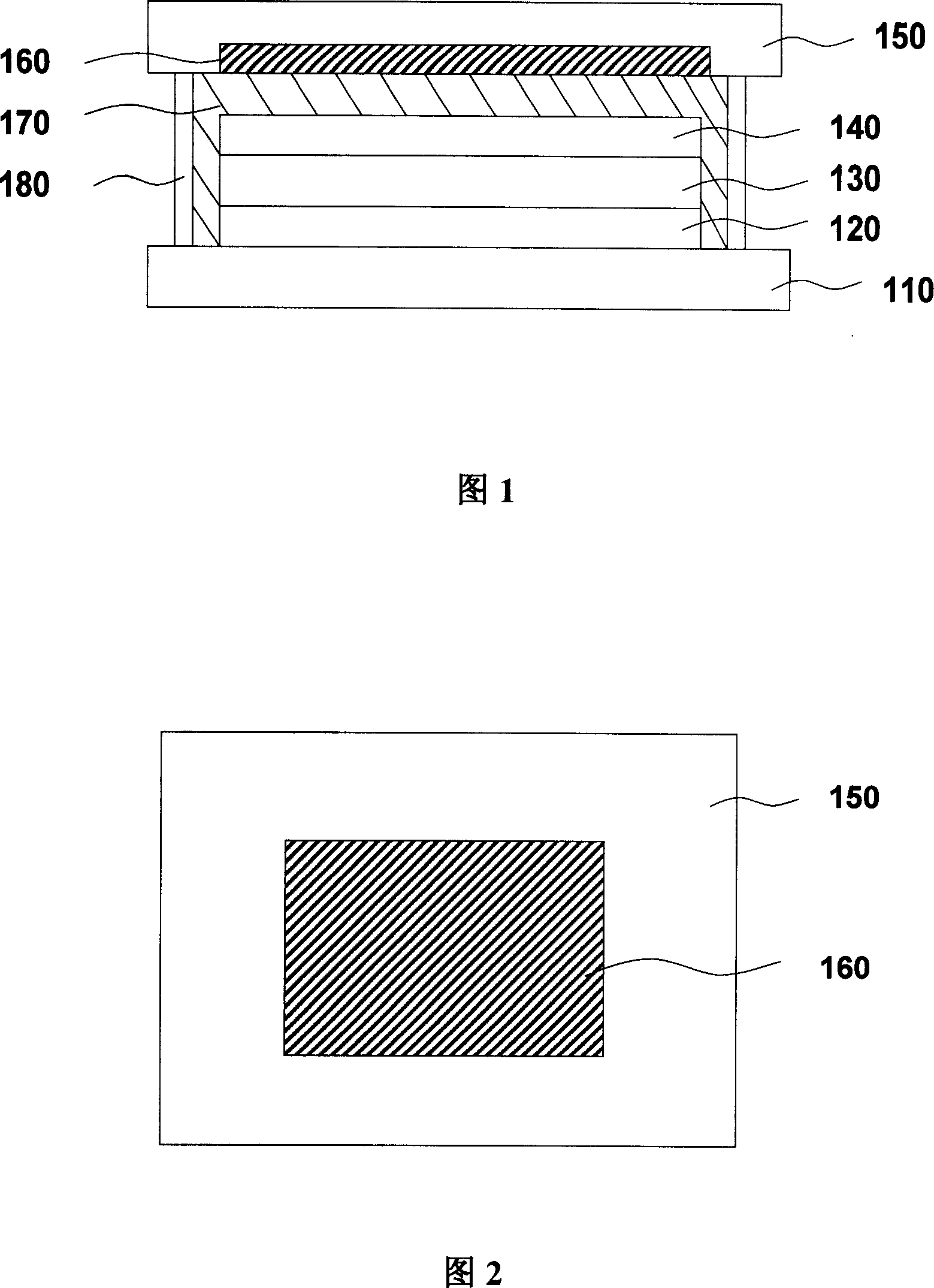
[0032] 1 is a cross-sectional view of the structure of the first embodiment of the organic light-emitting device of the present invention. An anode layer 120, a light-emitting layer 130, and a cathode layer 140 are sequentially arranged on a substrate 110, wherein the substrate 110 is generally a glass substrate, and the anode 120 is a transparent electrode. Metal oxides such as indium tin oxide (ITO), zinc oxide, and zinc tin oxide, or metals with higher work functions such as gold, copper, and silver, preferably ITO, and the light-emitting layer 130 may also include a hole injection layer, a hole transport layer, One or more layers of the electron injection layer and the electron transport layer. The hole transport layer is made of p-type organic semiconductor materials with strong hole transport ability, generally triphenylamine compounds, such as NPB, TPD, MTDATA and other materials. One, the electron transport layer is generally a metal-organic complex, such as Alq 3 , BA...

Embodiment 2

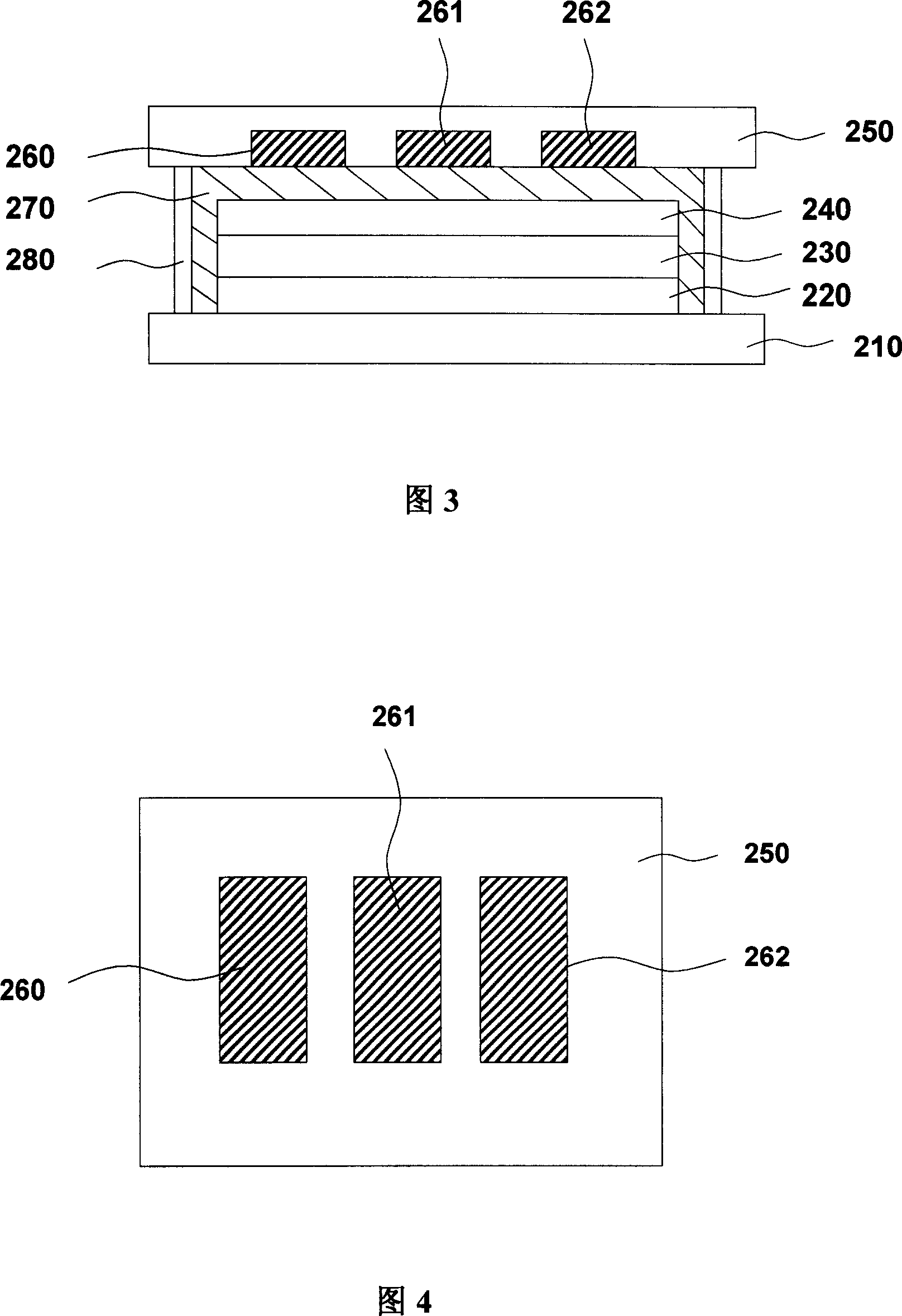
[0036]2 is a cross-sectional view of the structure of the second embodiment of the organic light-emitting device of the present invention. An anode layer 220, a light-emitting layer 230, and a cathode layer 240 are sequentially arranged on a substrate 210. The material selection of each layer is the same as in Example 1, and the cathode layer 240 is arranged above. There is a packaging board 250, and the packaging board 250 and the substrate 210 are bonded and fixed by the packaging glue 280. The packaging board 250 contains three independent low-melting point metal layers 260, 261 and 262, which are respectively filled with metals with different melting points. In this embodiment, glass is selected as the packaging plate. During preparation, three cube-shaped grooves are sequentially formed on a plane inside the glass plate by means of stamping. The plan view of the structure is shown in Figure 4. Load three kinds of metal particles with different melting points, and then use ...

Embodiment 3

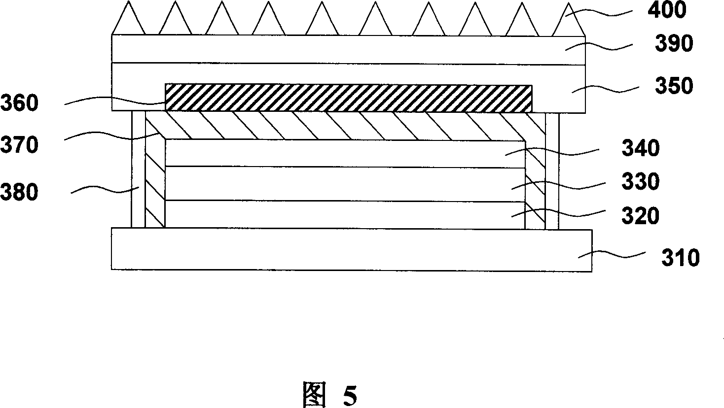
[0039] 3 is a cross-sectional view of the structure of the third embodiment of the organic light-emitting device of the present invention. An anode 320, a light-emitting layer 330, and a cathode 340 are sequentially arranged on a substrate 310. The selection of materials for each layer is the same as in Example 1, including a low-melting point metal layer 360. The packaging board 350 is arranged on the cathode layer 340, and the packaging board 350 and the substrate 310 are bonded and packaged by the packaging adhesive 380. The difference from Embodiment 1 and Embodiment 2 lies in the outer side of the packaging board 350 of this embodiment Also be provided with a metal heat dissipation plate 390 with heat dissipation protrusions 400, the metal heat dissipation plate 390 is a thermally conductive material, and its function is to help transfer the heat inside the device to the external environment better, and the heat dissipation protrusions 400 The effect is to increase the sur...


PUM

PropertyMeasurementUnit
melting pointaaaaaaaaaa

Abstract

The invention relates to a organic luminophor that includes base plate, anode layer, lightening layer, cathode layer and encapsulation plate which is used in encapsulation, it characterized in that said encapsulation plate possesses low melting point metal structure and function of radiating, said low melting point metal is embedded in cavity of said encapsulation plate, and encapsulated to inner of encapsulation plate by ultraviolet radiation solidify glue, the heat conduction material which possesses function of heat conduction is filled to the space between the cathode layer and the encapsulation plate, the invention, the craft of organic luminophor is simple, and the invention possesses perfect function of heat-conducting and radiating.

Description

technical field [0001] The invention relates to the field of organic electroluminescence, in particular to an organic electroluminescence device with an excellent heat dissipation structure. Background technique [0002] Organic light-emitting diodes (OLEDs) have great application potential due to their advantages such as self-illumination, wide viewing angle, power saving, easy manufacturing process, low cost, high response speed, and full color, and are expected to become an alternative to CRT, LCD, etc. High-profile next-generation flat-panel displays. [0003] Organic light-emitting diodes are white light-emitting elements, which will generate heat when emitting light. The heat energy accumulated between the substrate and the packaging board or between the substrate and the light-emitting layer will seriously reduce the luminous efficiency and uniformity of OLED elements. The structural design of existing devices And the heat dissipation of the packaging structure is po...

Claims


Application Information

Patent Timeline
Patent Type & Authority Applications(China)
IPC IPC(8): H01L51/50H01L51/52H01L51/54
Inventor 邱勇谢静高裕弟范晓毅
Owner GUAN YEOLIGHT TECH CO LTD
Why Eureka
Try Eureka