III nitride semi-conductor material and growing method thereof

A nitride semiconductor and growth method technology, which is applied in the directions of semiconductor devices, semiconductor/solid-state device manufacturing, and semiconductor/solid-state device components, etc., can solve the problems of vertical sidewall inclination of grooves, increased manufacturing costs, and epitaxial growth failures, etc. Achieve the effect of easy peeling and lower growth cost

Inactive Publication Date: 2008-03-12
MAANSHAN JASON SEMICON CO LTD
View PDF0 Cites 6 Cited by
  • Summary
  • Abstract
  • Description
  • Claims
  • Application Information

AI Technical Summary

Problems solved by technology

[0011] Although the etching lateral epitaxy method avoids the disadvantages of the mask, it is very difficult to etch on chemically and physically corrosion-resistant materials such as sapphire and silicon carbide, which leads to increased manufacturin

Method used


Image

  • III nitride semi-conductor material and growing method thereof
  • III nitride semi-conductor material and growing method thereof
  • III nitride semi-conductor material and growing method thereof

Examples


Embodiment 1

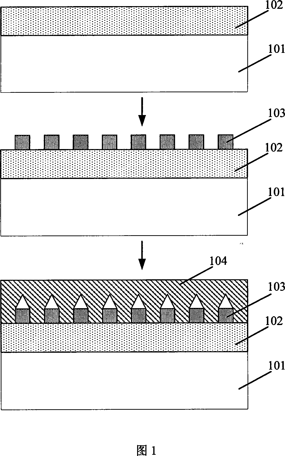
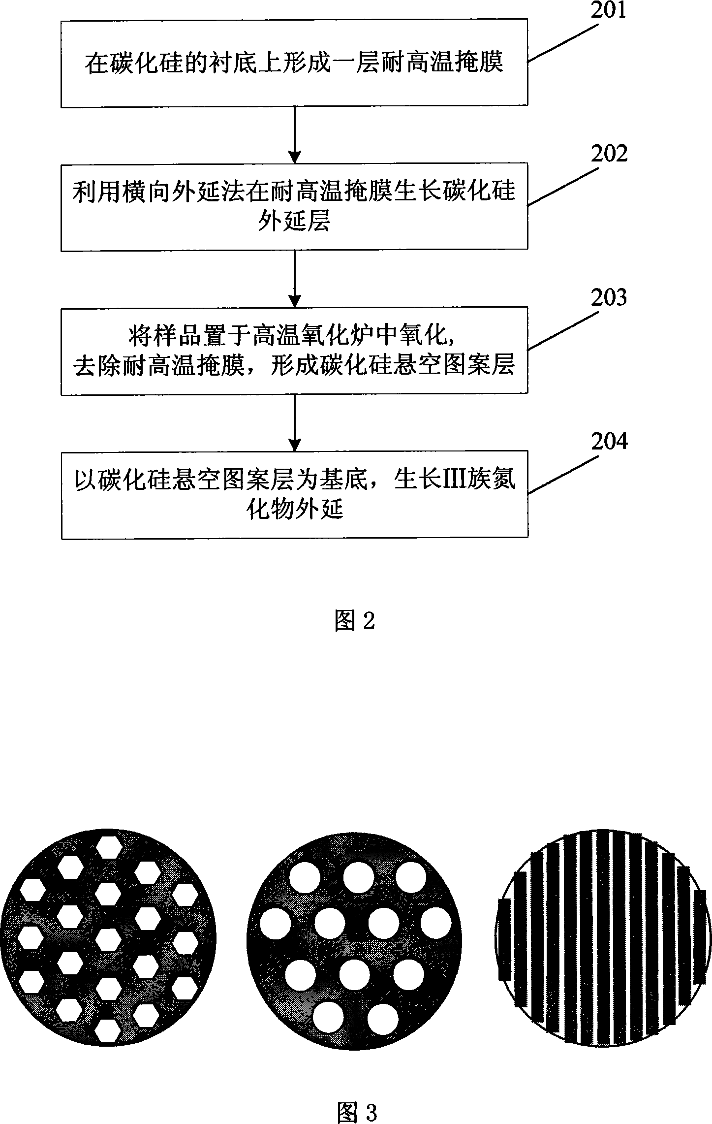
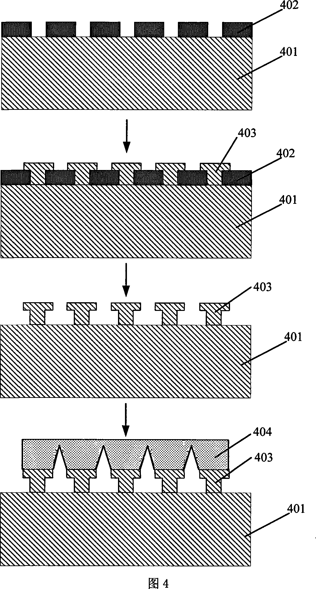
[0047] This embodiment provides a method for growing a Group III nitride semiconductor material, including:

[0048] First, a layer of high-temperature resistant mask is formed on the semiconductor substrate; then, an epitaxial layer homogeneous to the upper substrate is grown on the high-temperature resistant mask by lateral epitaxy; and then the above-mentioned semiconductor is placed in a high-temperature oxidation furnace Oxidation, removing the high-temperature resistant mask, forming a heterogeneous suspended pattern layer that is homogeneous with the above substrate or with a lattice matching coefficient of less than 3%; then, using the suspended pattern layer as a base, grow III-nitride epitaxy to form a III-group Nitride semiconductor materials.

[0049] Among them, group III nitrides include gallium nitride, aluminum nitride, aluminum gallium nitride, indium gallium nitride and aluminum indium gallium nitride, etc., and the substrate is usually silicon carbide, silic...

Embodiment 2

[0063] This embodiment provides a Group III nitride semiconductor material, which is grown by the method provided in Embodiment 1. Referring to FIG. 5 , the Group III nitride semiconductor material includes:

[0064] substrate 501;

[0065] The suspended pattern layer 502 is formed on the substrate 501 by epitaxy, and the material of the suspended pattern layer 502 is the same as that of the substrate 501;

[0066] The III-nitride epitaxy 503 is grown on the suspended pattern layer 502 by the III-nitride epitaxy technique.

[0067] Wherein, the substrate 501 is: silicon carbide, silicon, gallium arsenide or zinc oxide.

[0068] The advantages of the above technical solutions are as follows:

[0069] Due to the growth characteristics of PVT, the quality and surface polishing requirements of SiC are reduced, thereby reducing the growth cost; at the same time, since PVT itself is a low-cost growth method, the growth cost can be further reduced.

[0070] The lateral growth rate...


PUM


Abstract

The invention discloses a semiconductor material for nitride of group III and its growing directions, which belongs to the field of semiconductor technology. The said method is composed of: forming a heat-resistant mask layer on the semiconductor substrate; growing the epilayer homogeneous with the said substrate on the said heat-resistant mask layer by epitaxial method; oxidize the said semiconductor into the oxidation furnace and eliminate the heat-resistant mask to form impending pattern homogeneous with the said substrate; Taking the said impending pattern as the base, growing the epitaxis of the nitride of group III to form the semiconductor material for nitride of group III, which comprises a substrate, impending pattern on the base of the substrate formed by epitaxial technology and the epitaxis of the nitride of group III on the impending pattern by epitaxial technology of the nitride of group III. The invention lowers the growing cost and reduces the stress between growing-finishing grown film and substrate through the impending pattern, thus to grow flawless thick film.

Description

technical field [0001] The invention relates to the field of semiconductor technology, in particular to a Group III nitride semiconductor material and a growth method thereof. Background technique [0002] Aluminum nitride (AlN), gallium nitride (GaN), indium nitride (InN) and their ternary or quaternary alloys are usually called III-nitrides. At present, the epitaxial growth of III-nitrides has not yet been developed. Available mature and stable commercial homoepitaxial substrates. Products based on group III nitrides, such as blue and green light emitting diodes (LED, Light Emitting Diode), high electron mobility transistors (HEMT, High Electron Mobility Transistor), etc., are all realized through heteroepitaxy. At present, the general heterogeneous substrates of III-nitrides include sapphire (Sapphire), silicon carbide (SiC), silicon (Si), gallium arsenide (GaAs), etc. III-nitrides and their lattice and thermal mismatch It inevitably leads to high-density crystal defect...

Claims


Application Information

Patent Timeline
IPC IPC(8): H01L21/20H01L23/00
Inventor 高英张剑平周瓴武帅
Owner MAANSHAN JASON SEMICON CO LTD
Why Eureka
Try Eureka