Silicon chip etching method

A silicon wafer and etching technology, which is used in electrical components, semiconductor/solid-state device manufacturing, circuits, etc., can solve the problem of rough surface of the sidewall of the etching groove, difficult to guarantee the characteristic structure of etching, and ineffectiveness of the sidewall of the etching groove. Ground protection and other issues, to achieve the effect of smooth sidewalls, smooth edges, and obvious structural features

Active Publication Date: 2008-03-26
BEIJING NAURA MICROELECTRONICS EQUIP CO LTD
View PDF0 Cites 16 Cited by
  • Summary
  • Abstract
  • Description
  • Claims
  • Application Information

AI Technical Summary

Problems solved by technology

During the polysilicon etching process, this kind of process gas has a high vapor pressure of the reaction product, which is easy to volatilize into the gas phase and be discharged as a gas, so it has a faster etching rate, but at the same time, the protection formed on the side wall of the etching groove The layer material is also easy to break away from the surface of the

Method used


Image

  • Silicon chip etching method

Examples


Example Embodiment

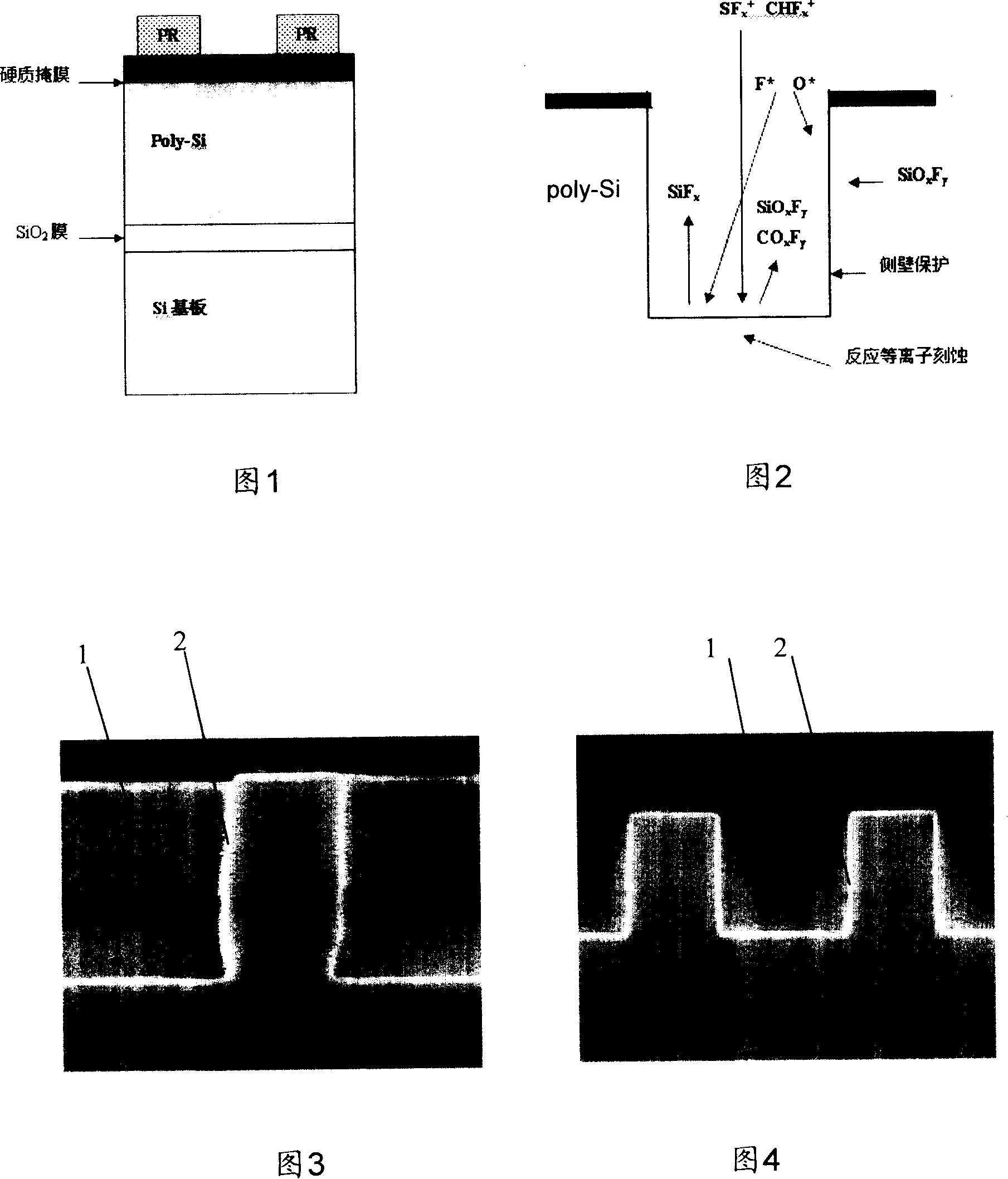
[0029] The present invention is mainly used to etch silicon wafers, and its preferred specific implementation is to include three steps of preliminary etching, main etching, and over-etching. The purpose of the preliminary etching step is to remove the hard mask above the silicon wafer layer. For the film layer or other dielectric layers, the main etching step realizes the etching of the silicon wafer, and the purpose of the over-etching step is to further etch the silicon wafer layer to achieve a complete etching of the silicon wafer layer.

[0030] The following takes the etching of polysilicon as an example to specifically describe the implementation process of the present invention:

[0031] Polysilicon is an important area in the multilayer structure of integrated circuits, and its patterned etching quality will have a direct impact on the subsequent process flow.

[0032] As shown in Figure 1, MOSFET (metal-oxide semiconductor field effect transistor) is a representative ins...


PUM


Abstract

The silicon chip etching process includes three steps including an initial etching, a main etching and a post etching. The main etching step adopts technological gas of CHF3, O2 and SF6 mixture in the flow rate of 10-500 sccm and pressure of 4-100 material; an upper RF power source SFR to ionize the gas mixture filled into the reaction cavity into plasma and a lower RF power source BFR to accelerate the plasma bombarding the surface of the silicon chip. In the step, F* free radical and Si react to form SiFx; SiFx is oxidized by O2 in the gas mixture to form SiOxFy attached to the side wall of the etched channel to constitute a protecting layer and to make the etched side wall smooth and flat. The process is suitable for etching silicon chips of all types, especially polycrystalline silicon layer in line width smaller than 90 nm.

Description

technical field [0001] The invention relates to a semiconductor silicon chip processing technology, in particular to a silicon chip etching process. Background technique [0002] At present, microelectronic technology has entered the era of VLSI and system integration, and microelectronic technology has become the symbol and foundation of the entire information age. [0003] In microelectronics technology, to manufacture an integrated circuit, it needs to go through several processes such as integrated circuit design, mask manufacturing, raw material manufacturing, chip processing, packaging, and testing. In this process, etching the semiconductor silicon wafer to form process trenches is the key technology. [0004] Commonly used etching methods include wet etching and dry etching. Wet etching refers to the method of etching by chemical reaction using liquid chemical reagents or solutions; dry etching mainly uses low-voltage discharge The ions or radicals (molecules, atom...

Claims


Application Information

Patent Timeline
IPC IPC(8): C23F1/12C23F4/00H01L21/306H01L21/3065
Inventor 尹海涛
Owner BEIJING NAURA MICROELECTRONICS EQUIP CO LTD
Why Eureka
Try Eureka