Making method for organic thin film transistor

A manufacturing method and organic thin film technology, applied in semiconductor/solid-state device manufacturing, electrical solid-state devices, semiconductor devices, etc., can solve problems such as poor stability, difficult to reach, difficult to dissolve, etc., and achieve the effect of device performance improvement

Inactive Publication Date: 2008-05-28
BEIJING JIAOTONG UNIV
View PDF0 Cites 11 Cited by
  • Summary
  • Abstract
  • Description
  • Claims
  • Application Information

AI Technical Summary

Problems solved by technology

[0003] However, in the production process of large-scale integrated circuits of these flexible substrates, the steps of lithography process and vacuum preparation process (for example: PVD, CVD, etc.) are used many times, so it is difficult to reduce the cost of device preparation. In the past, roll-to-roll (R2R) was used for large-scale production, and the research on solution-prepared organic thin film transistors began. Most of them used polymer organics for printing and spin coating to reduce production costs, but it was difficult to achieve high mobility and stability. is also poor, making it difficult to improve device performance
However, pentacene and polythiophene oligomers with high mobility are insoluble and unstable, so it is difficult to directly use them for printing and spin coating to prepare transistors.

Method used


Image

  • Making method for organic thin film transistor
  • Making method for organic thin film transistor
  • Making method for organic thin film transistor

Examples


Embodiment 1

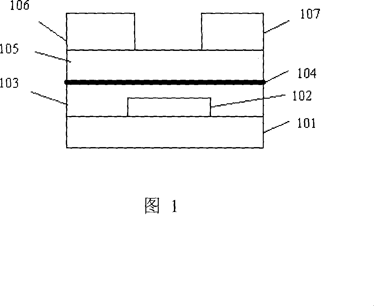
[0027] Step 1, cleaning the ITO glass sheet corroded with hydrochloric acid, the glass sheet is used as the substrate 101, and the ITO is used as the grid 102;

[0028] Step 2, plating silicon dioxide with a thickness of 250 nanometers on the ITO as the gate insulating layer 103;

[0029] The SD400M-MULTISOURCE ORGANICMOLECULAR VAPOR DEPOSITION SYSTEM inorganic coating equipment and NG-3 electron beam evaporation power supply produced by Shenyang Star Vacuum Technology Application Research Institute were used to prepare silicon dioxide films; coating conditions: system vacuum degree 9.8E-4Pa, Foreline vacuum degree 1.OEOPa, growth rate 1 Ȧ / S, deposition time 45 minutes;

[0030] Step 3, transfer the sample treated in step 2 to 2wt% OTS solution (octadecyltrichlorosilane Acros-14740, octadecyltrichlorosilane, molecular formula is C 18 h 37 SiCl 3 , prepared with hexadecane) for 4 hours to form a self-assembled monolayer 104 on the gate insulating layer 103;

[0031] Step 4,...

Embodiment 2

[0038] The other steps are the same as in Example 1, except that the method of forming the self-assembled monolayer 104 on the gate insulating layer 103 is different; using a DEL multifunctional high vacuum system, it is prepared by thermal evaporation, and a few drops of 2wt% The OTS solution is pre-pumped so that the vacuum degree of the chamber is less than 3E-3Pa, and the vapor phase is deposited on the plated silicon dioxide. After 15 minutes of deposition, a self-assembled monolayer 104 is formed on the gate insulating layer 103 .

Embodiment 3

[0040] Other steps are the same as in Embodiment 1, the difference is that the material and formation method of the organic semiconductor layer 105 are different; the coating process of the organic semiconductor layer is carried out, and the pentacene derivative TES thienyl pentacene of the 6,13-substituent is used. Benzene, with the formula

[0041]

[0042] Prepare a 4wt% toluene solution, spin-coat at 2000rpm for 60 seconds and deposit on the sheet, then anneal in air at 90°C for 2 minutes, the precursor of the pentacene derivative is converted into a pentacene film, and the organic semiconductor layer 105 is obtained. .

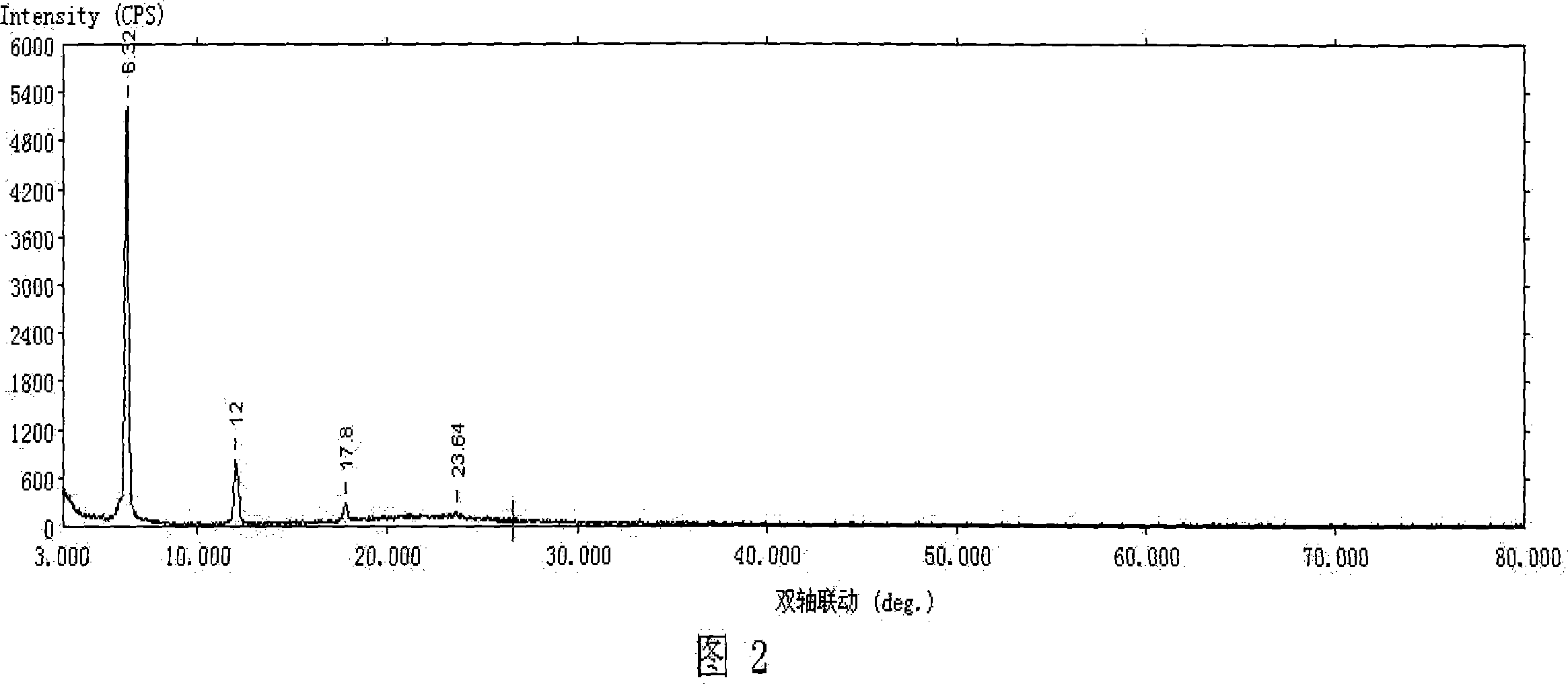
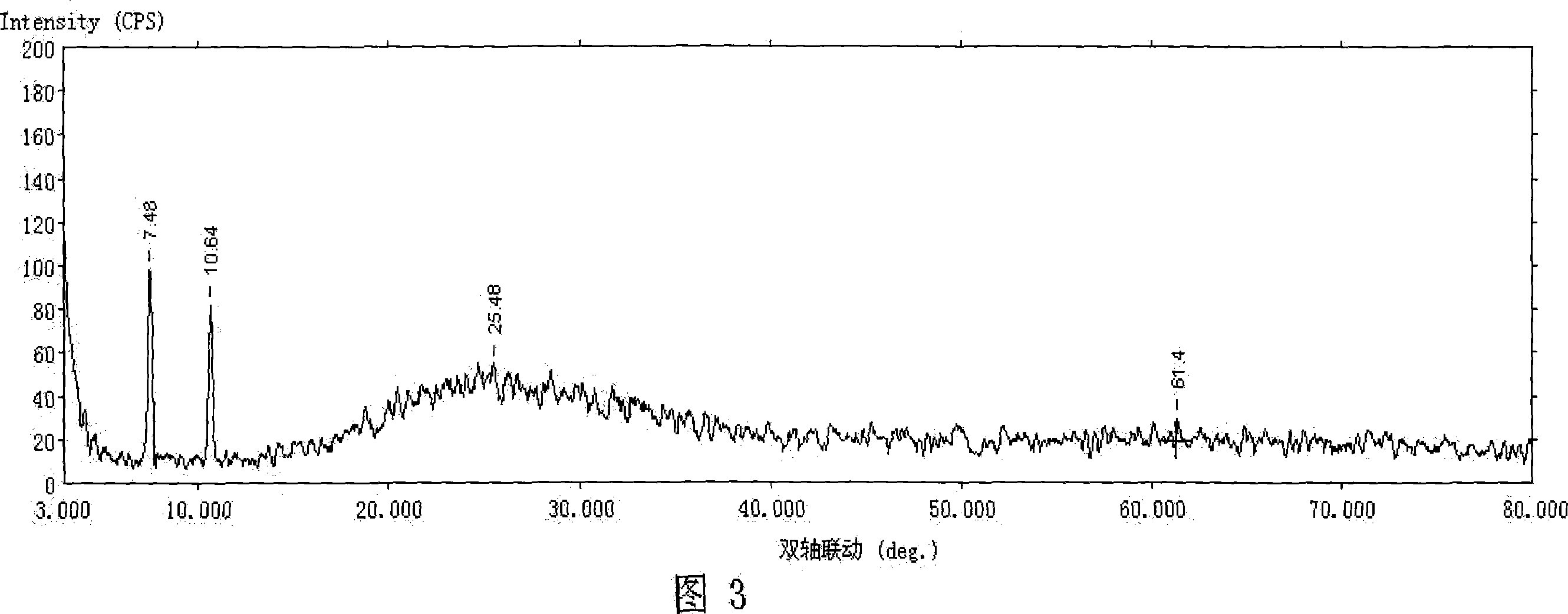
[0043] Using the KEITHLEY 2410 source unit I-V test system to measure the I-V characteristic curve of organic thin film transistor devices, it is obtained that at different gate voltages V GS Next, the source-drain current I DS vs. source-drain voltage V DS The I-V relationship map, and then calculate the mobility in the saturation region according ...


PUM


Abstract

The invention relates to a manufacturing method of an organic thin-film transistor, which is suitable for the fields of the display, the sensor, the radio frequency identification (RFID) of a label, etc. The organic thin-film transistor has the structure that a grid (102), a gate insulator layer (103), a source cathode (104), a drain (105), a surface modification layer (106) and an organic semiconductor layer are arranged on a basement (101) in sequence. The preparation of the organic semiconductor layer can be realized via the transformation of pentacene derivatives to pentacene crystal. Through the adoption of the method, the organic semiconductor material is spin-coated and printed in a large area via solution. The manufacture of the organic thin-film transistor in large scale integration with a flexible substrate is accomplished, and the manufacture cost of the integrated circuit with the organic thin-film transistor can be reduced. Simultaneously, the surface modification layer is formed in the source cathode and the drain via OTS solution. The high mobility of the organic thin-film transistor, low leakage current and circuit working voltage can be further guaranteed.

Description

technical field [0001] The invention relates to a method for manufacturing an organic thin film transistor. Suitable for displays, sensors, radio frequency identification (RFID) tags and other fields. Background technique [0002] Flexible substrates, low cost, and low-temperature processes have greatly improved the opportunities for organic thin-film transistors (OTFTs) to be applied to large-area flexible electronic products. At the same time, organic integrated circuits can also be fabricated on cheap plastic substrates. , Form printed circuits, replace silicon chips, and can be mass-produced by printing, so that displays, sensors, smart cards, and radio frequency identification (RFID) tags can be brought to the market on a large scale. [0003] However, in the production process of large-scale integrated circuits of these flexible substrates, the steps of lithography process and vacuum preparation process (for example: PVD, CVD, etc.) are used many times, so it is diffi...

Claims


Application Information

Patent Timeline
Patent Type & Authority Applications(China)
IPC IPC(8): H01L51/40
Inventor 徐征田雪雁赵谡玲张福俊袁广才
Owner BEIJING JIAOTONG UNIV
Why Eureka
Try Eureka