Nano tin soldering method by using atomic force microscopy probe as welding gun
Atomic force microscopy, atomic force microscopy technology, applied in nanotechnology, nanotechnology, nanostructure manufacturing and other directions, can solve the problems affecting the overall performance of the device, the large difference in redox potential, etc., which is conducive to industrialization, accurate positioning, Universal effect
- Summary
- Abstract
- Description
- Claims
- Application Information
AI Technical Summary
Problems solved by technology
Method used
Image

Examples
Embodiment 1
[0024] Example 1: Using ZnO sol as solder, implement nano-welding on a silicon wafer to obtain a 2×2 array
[0025] (1) Preparation of solder: with Zn(OAc) 2 2H 2 O as a precursor of ZnO. Zn(OAc) 2 2H 2 O was dissolved in isopropanol, and a small amount of twice distilled water was added dropwise under the action of the stabilizer diethanolamine. After fully stirring and hydrolyzing, a transparent ZnO sol was obtained, and the solubility of the sol was 0.5mol / L.
[0026] (2) Nano-solder dipping: Use a pipette gun to take 10 μL of the above-mentioned zinc oxide sol, drop it on the newly cleaved mica sheet, dip the AFM probe into the solder, and let the tip stand for 5 minutes.
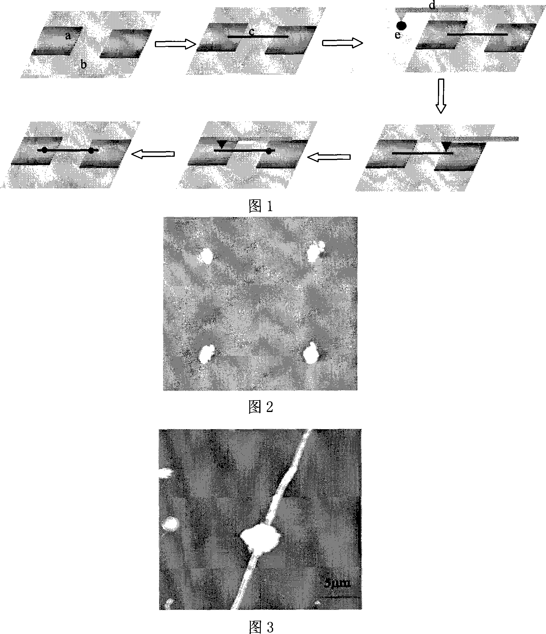
[0027] (3) Welding implementation: using contact mode imaging technology, select a certain area on the pre-treated silicon wafer for imaging, and record the image. Reduce the scanning range to 50nm, and then apply a certain bias voltage on the probe to make the tip touch the surface, keep the scann...
Embodiment 2
[0030] Embodiment 2 uses ZnO sol as the soldering tin to the welding of zinc oxide nanowires
[0031] The preparation of the solder and the solder dipping of the AFM probe are basically the same as in Example 1. Before implementing soldering, it is first necessary to detect whether the zinc oxide nanowires spin-coated on the silicon wafer are single dispersed. Select a zinc oxide nanowire as the target we want to weld, and get its height image. After the AFM probe is dipped in solder, after standing for 20 minutes, the AFM scans to find the zinc oxide nanowires to be welded, and records the height image. The implementation of the welding process still adopts the contact mode, and the specific operation process is as described in step (3) of embodiment 1. Figure 3 is an AFM picture of a single ZnO nanowire welded by an AFM probe. It can be seen from the figure that the positioning of the soldering point is accurate, and the amount of soldering tin is well controlled.
Embodiment 3
[0032] Embodiment 3 uses silver ammonia solution as solder, adopts AFM probe non-contact mode to implement nano welding
[0033] Based on the traditional silver mirror reaction as the theoretical basis, the introduction of gas phase reaction in technical implementation simplifies the actual operation.
[0034] The specific implementation process is as follows:
[0035] (1) Preparation of solder: add 2% NH 4 OH aqueous solution was added dropwise to 2% AgNO 3In the solution, silver ammonia solution is obtained, and the pH is adjusted to 10 with NaOH, which is used as solder for nano-welding. The silicon wafer is used as the substrate, and the monodisperse single-walled carbon nanotubes placed on the silicon wafer are used as the welding object, and the AFM tapping mode imaging is used to image the carbon nanotubes to be welded.
[0036] (2) Nano-solder dipping: Select the NSC11 tip as the welding torch, dip an appropriate amount of solder (silver-ammonia solution), let it st...
PUM
| Property | Measurement | Unit |
|---|---|---|
| Diameter | aaaaa | aaaaa |
Abstract
Description
Claims
Application Information
 - Generate Ideas
- Intellectual Property
- Life Sciences
- Materials
- Tech Scout
- Unparalleled Data Quality
- Higher Quality Content
- 60% Fewer Hallucinations
Browse by: Latest US Patents, China's latest patents, Technical Efficacy Thesaurus, Application Domain, Technology Topic, Popular Technical Reports.
© 2025 PatSnap. All rights reserved.Legal|Privacy policy|Modern Slavery Act Transparency Statement|Sitemap|About US| Contact US: help@patsnap.com