Two-dimensional ordered organic semiconductor composite nano membrane as well as special substrate and preparation method thereof

An organic semiconductor and thin film technology, which is applied in the field of two-dimensional ordered organic semiconductor composite nano-films and their special substrates and their preparation, can solve the problems of reducing the bulk properties of organic semiconductor materials, hindering the practical application of organic semiconductors, etc., and achieves a preparation method. Simple, low-cost, performance-improving effect

Inactive Publication Date: 2008-07-30
INST OF CHEM CHINESE ACAD OF SCI
View PDF0 Cites 17 Cited by
  • Summary
  • Abstract
  • Description
  • Claims
  • Application Information

AI Technical Summary

Problems solved by technology

[0003] However, in all known techniques for preparing organic semiconductor thin films so far, since the substrates used are mostly in an amorphous state, the thin film materials prepared on the surface of these amorphous substrates are microscopically ordered locally, but Macroscopically, it is in a disordered state as a whole, which greatly reduces the bulk performance of organic semiconductor materials, thus hindering the practical application of these organic semiconductors as film materials.

Method used


Image

  • Two-dimensional ordered organic semiconductor composite nano membrane as well as special substrate and preparation method thereof
  • Two-dimensional ordered organic semiconductor composite nano membrane as well as special substrate and preparation method thereof
  • Two-dimensional ordered organic semiconductor composite nano membrane as well as special substrate and preparation method thereof

Examples


Embodiment 1

[0030] Embodiment 1, preparation polymer dielectric ultra-thin film

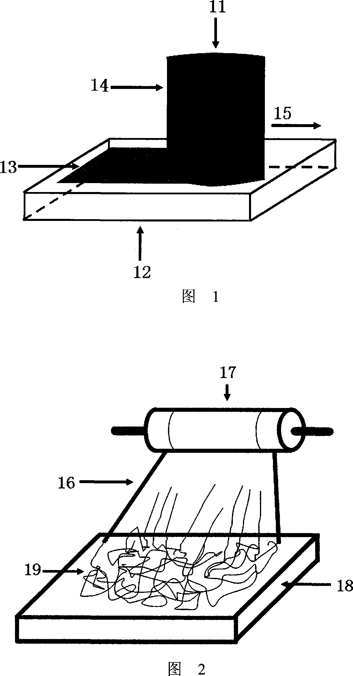
[0031] As shown in Figure 1, the method for preparing polytetrafluoroethylene (PTFE) dielectric ultra-thin film 13 by friction method is to preheat the glass substrate 12 (the glass substrate soaked in alkaline solution and cleaned with deionized water) to 280°C After that, apply a downward pressure 11 of 100N perpendicular to the glass substrate 12 to the polytetrafluoroethylene 14 placed on the glass substrate 12, and apply a uniform thrust of 10N along the horizontal direction, so that the polytetrafluoroethylene 14 is placed on the glass substrate 12 Extend horizontally at a speed of 15 cm / s to obtain an oriented polytetrafluoroethylene dielectric ultra-thin film 13 along the rubbing direction 15 .

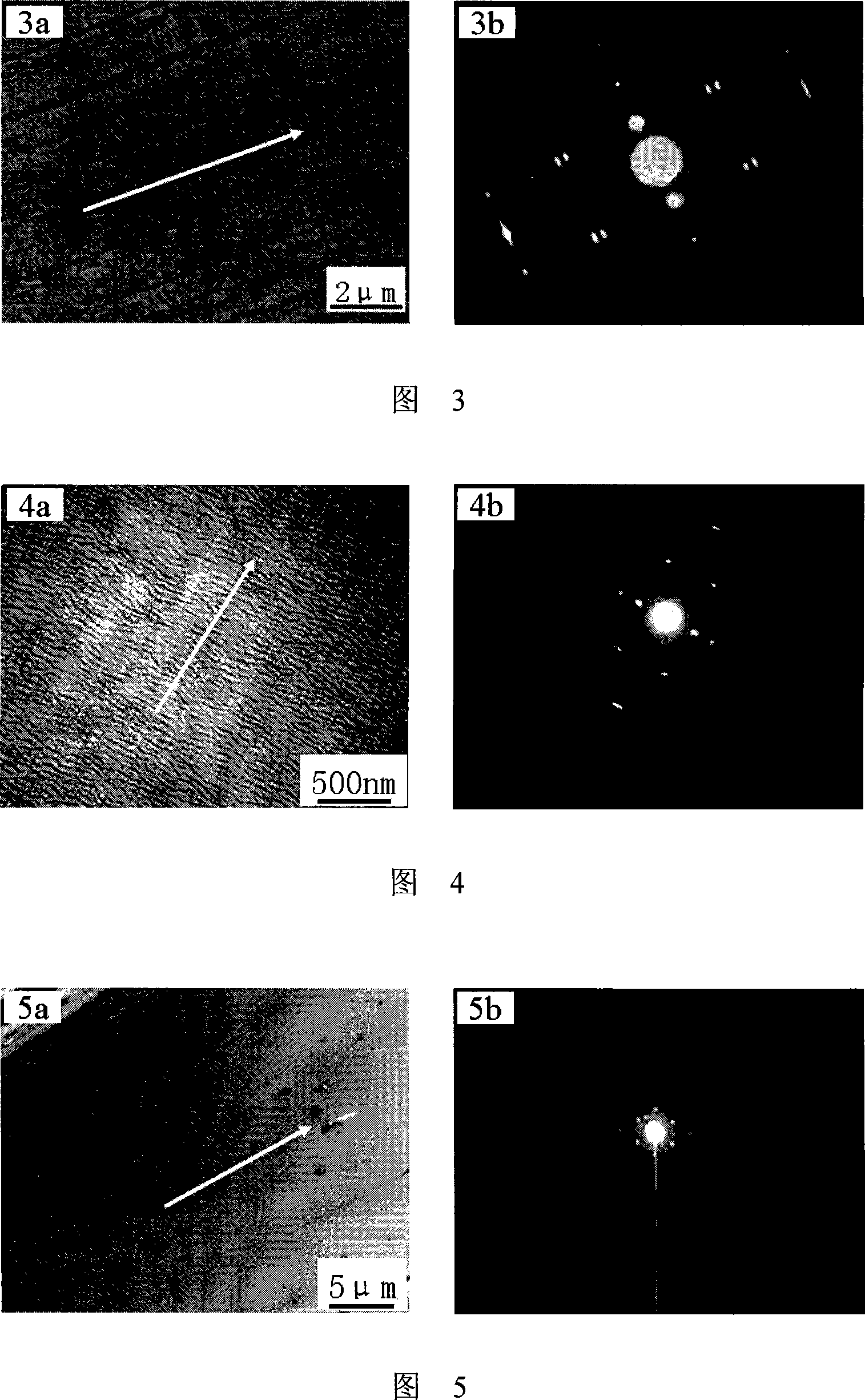
[0032] After measurement, it can be known that the thickness of the polytetrafluoroethylene dielectric ultra-thin film is about 60-120nm. Figure 3a and Figure 3b are the transmission electron microscope bri...

Embodiment 2

[0033] Embodiment 2, preparation polymer dielectric ultra-thin film

[0034] As shown in Figure 2, the method of preparing polymer dielectric ultra-thin films by melt stretching method is to mix polyethylene with xylene, heat and stir to fully dissolve, and prepare 0.5 grams of polyethylene per 100 milliliters of xylene homogeneous solution, and then evenly apply the homogeneous solution to the flat and smooth template 18 (glass plate) that has been preheated to 125 ° C. After the xylene is completely volatilized, a polyethylene melt film 19 is obtained. The mechanical roller 17 with adjustable rotating speed sticks the above-mentioned polyethylene melt film 19 and draws and stretches it; Attached to an alternate substrate (which is a silicon wafer). Wherein, the coefficient of friction of the mechanical roller used is 0.5.

[0035]After measurement, it can be known that the thickness of the polyethylene dielectric ultra-thin film is about 80-120nm. Figure 4a and Figure 4b ...

Embodiment 3

[0036] Example 3, preparation of two-dimensional ordered organic semiconductor composite nanofilm

[0037] The method for preparing a two-dimensional ordered organic semiconductor composite nano-film by the solution spin coating method provided by the present invention is to first prepare poly(2,5-dialkoxy-p-phenyleneethynylene) with a mass volume percentage concentration of 0.5 % (containing 0.5 g of poly(2,5-dialkoxy-p-phenyleneethynylene) per 100 ml of toluene) in 10 ml of toluene solution. At room temperature above-mentioned solution is spin-coated on the silicon chip substrate that has orientation polytetrafluoroethylene (PTFE) dielectric ultra-thin film that obtains by embodiment 1 again, and the spinning speed of film throwing machine is 2000 rev / mins, obtains that thickness is 50nm poly(2,5-dialkoxy p-phenyleneethynylene) organic semiconductor composite nano film.

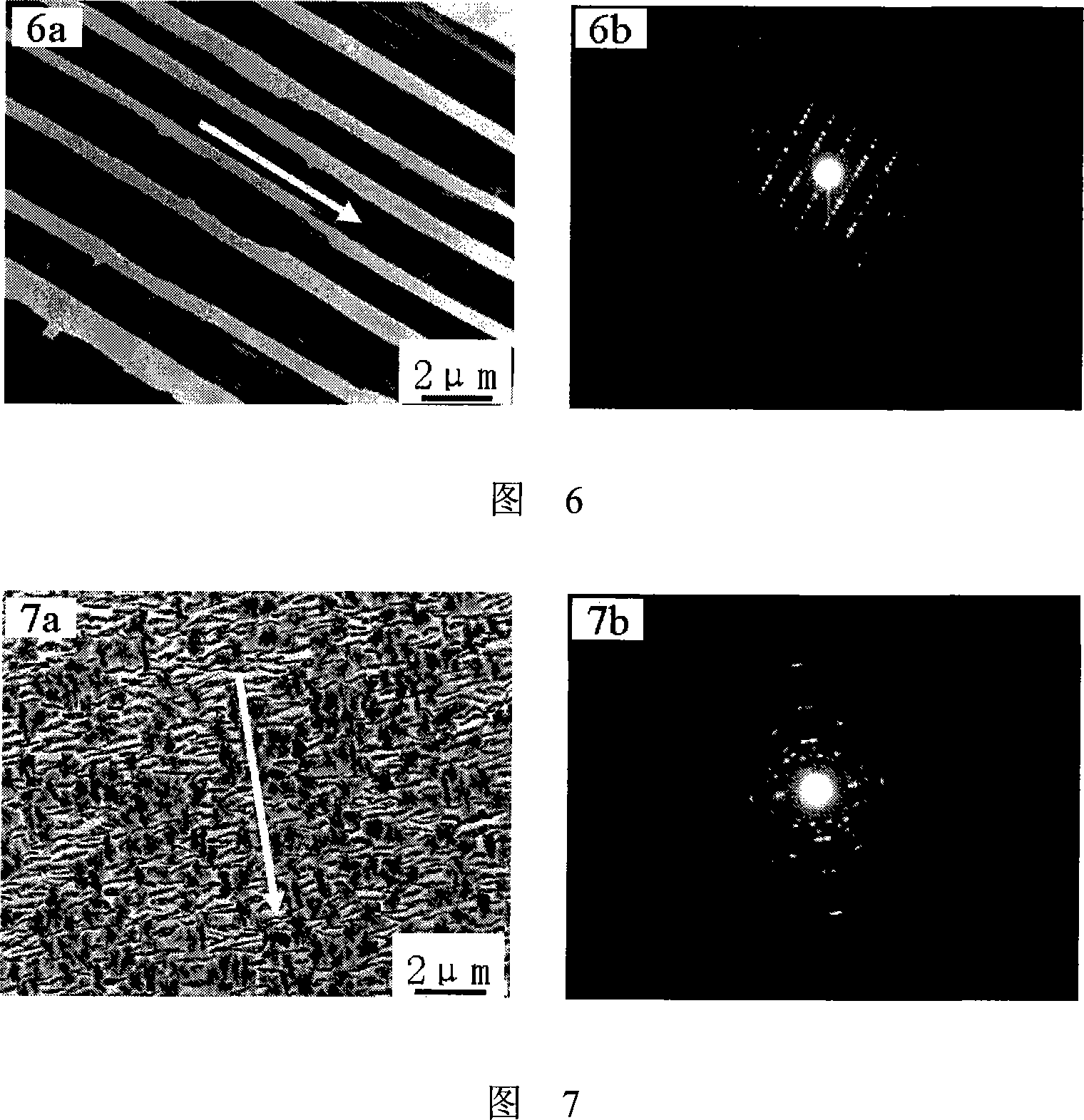
[0038] Observing the microstructure of the above-mentioned organic semiconductor composite nano-film pr...


PUM

PropertyMeasurementUnit
thicknessaaaaaaaaaa
thicknessaaaaaaaaaa
thicknessaaaaaaaaaa

Abstract

The invention discloses two-dimensional ordered organic semiconductor compound nanometer film and the special-purpose substrate thereof, and the preparation method thereof. Polymer dielectric ultra film provided by the invention is obtained by rubbing or stretching the polymer. The provided two-dimensional ordered organic semiconductor compound nanometer film is formed by compounding the polymer dielectric ultra film and the organic semiconductor compound nanometer film. Through adjusting and controlling the orientation degree, the thickness, the heating temperature, the solution spin coating speed and the vacuum evaporation coating speed of the pre orientated polymer dielectric ultra film, the two-dimensional ordered organic semiconductor compound nanometer film which can meet the ordered structure and the film thickness of different demands is prepared. The preparation method is simple and feasible, the efficiency is high, the cost is low, the performance of the thin film can be greatly improved, the stability is high, and the two-dimensional ordered organic semiconductor compound nanometer film can be used for the fields such as sensing material, electrical conduction material and electro-optical transformation material, etc.

Description

technical field [0001] The invention relates to the field of organic semiconductor thin film materials, in particular to a two-dimensional ordered organic semiconductor composite nano thin film, its special substrate and its preparation method. Background technique [0002] Compared with traditional silicon-based semiconductor materials, organic semiconductor materials can easily prepare nanometer-scale ultra-thin films through simple techniques such as solution spin coating, gas phase transport and vacuum evaporation, achieving larger areas at lower temperatures. Manufacturing, and the product has the characteristics of thinner, lighter and more flexible, and can achieve relatively simpler manufacturing process and lower production cost, so as to realize the lightweight, low cost and diversification of products in related application fields. [0003] However, in all known techniques for preparing organic semiconductor thin films so far, since the substrates used are mostly ...

Claims


Application Information

Patent Timeline
Patent Type & Authority Applications(China)
IPC IPC(8): C08J5/18C08L23/02C08L25/06C08L33/12C08L27/12C08L79/08C08L67/02C08L81/06C08L69/00C08J7/04B29C43/22B29C43/58B29C69/02B29C41/24B29C55/02H01L51/00B29L7/00
Inventor 闫寿科蒋士冬王朝晖胡文平董焕丽朱道本
Owner INST OF CHEM CHINESE ACAD OF SCI
Why Eureka
Try Eureka