

Method for preparing GaAs micro/nono optical element
A technology of optical elements and optical arrays, applied in optical elements, optics, microstructure technology, etc., can solve the problems of expensive and difficult, high processing costs, no low-cost micro/nano optical element processing methods, etc., and achieve high replication accuracy , The effect of low processing cost
- Summary
- Abstract
- Description
- Claims
- Application Information
AI Technical Summary
Problems solved by technology
Method used
Image

Examples
Embodiment 1
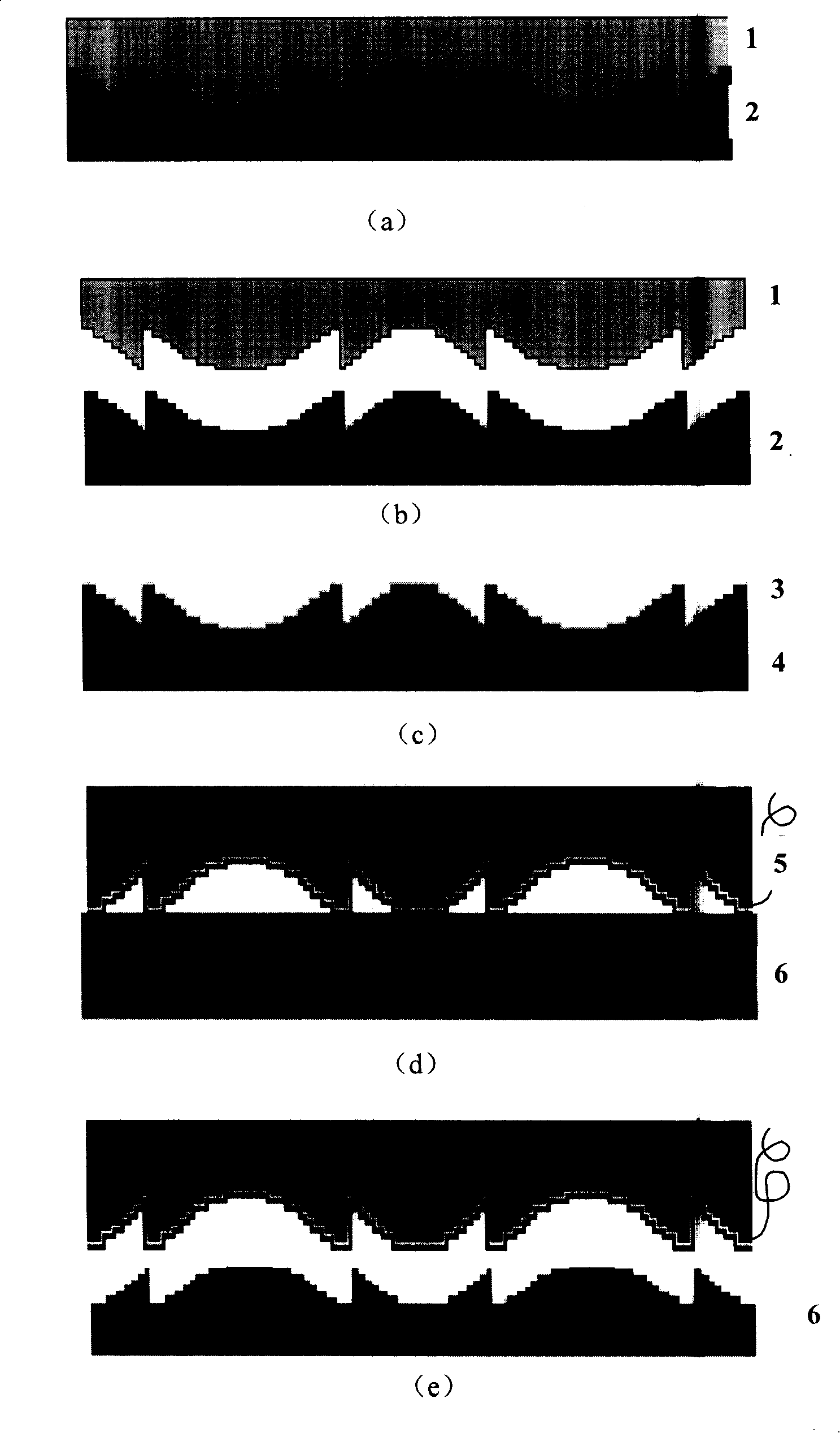
[0036] figure 1 A schematic diagram of the processing technology of Example 1 of the present invention is given.
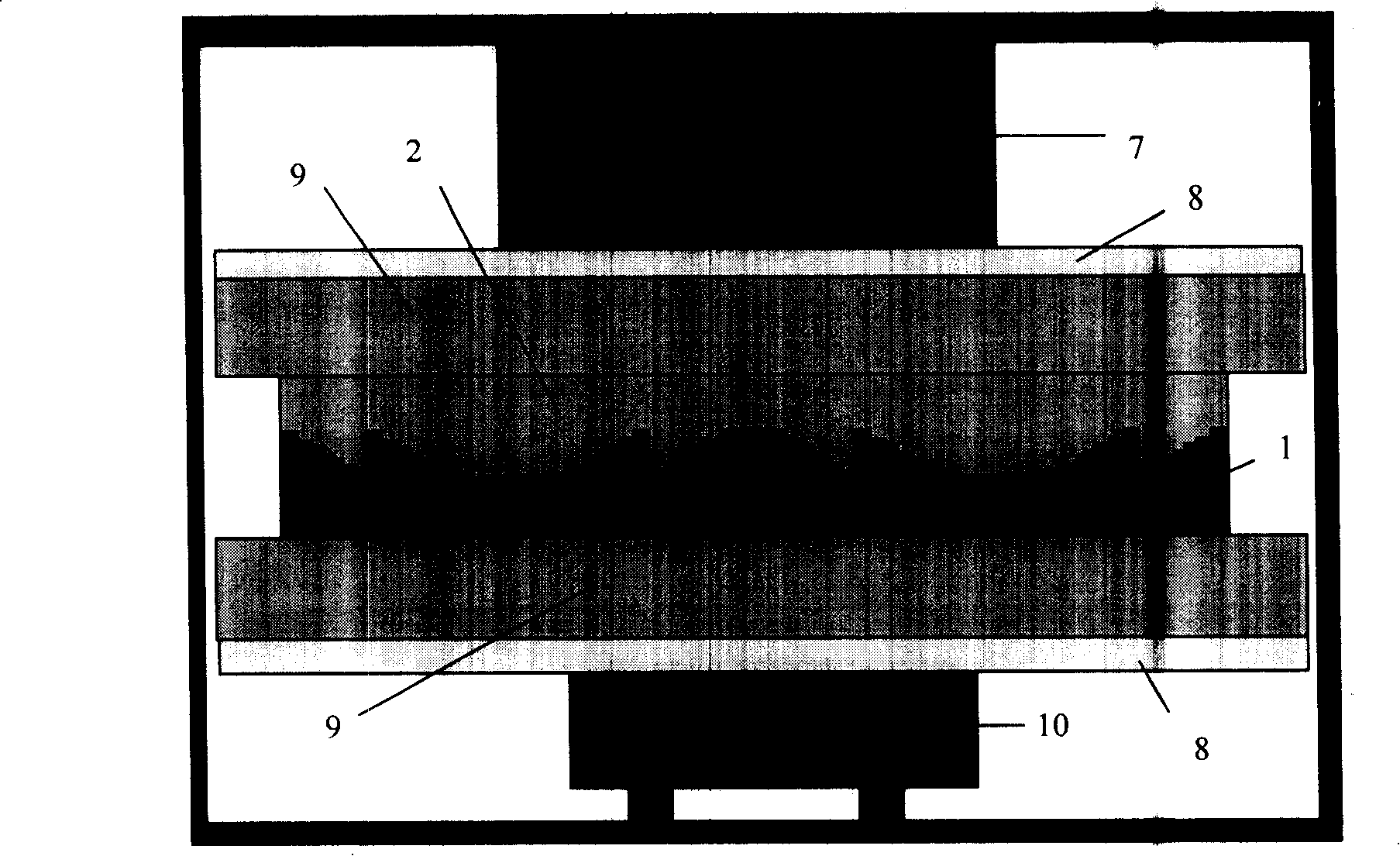
[0037] figure 1 a is the hot embossing process, the polymer material is PMMA 2 (polymethyl methacrylate) and the quartz optical element master 1 is placed in the hot embossing device, the selected glass transition temperature (T g ) temperature is 100°C. PMMA 2 has a thickness of 1mm and an area of 2cm 2 ,use figure 2 The shown hot embossing device is heated up to the glass transition temperature (T g ) above (generally controlled at 135°C), and then apply a pressure of 4 to 10 MPa for replication.
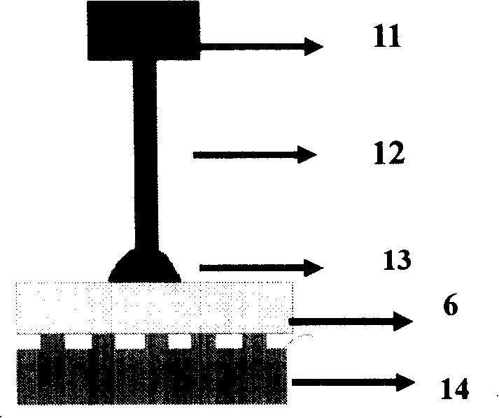
[0038] figure 1 B is the demoulding and separation process after hot pressing replication. After the hot pressed PMMA sheet 2 is separated from the quartz optical element master plate 1, the PMMA sheet 2 also needs to be degreased. 3 PO 4 50g / L+Na 2 CO 3 25g / L+NaOH 20g / L for degreasing treatment, the deoiling temperature is 85°C, and the time is 2.5h. ...
Embodiment 2-6
[0047] The specific operation steps of Examples 2-6 are the same as those of Example 1, and the specific composition of the solution is shown in Table 1, wherein the etching effect "+" is good.
[0048] Table 1
[0049] Example
PUM
 Abstract
Description
Claims
Application Information