A film LED chip part based on compound low-resistance buffer structure and its making method

A technology of LED chip and buffer structure, which is applied in the direction of semiconductor devices, electrical components, circuits, etc., can solve problems such as failure, cracking or structural changes, and achieve the effects of reducing chip warping, reducing production costs, and improving product yield

Active Publication Date: 2008-08-13
XIAMEN SANAN OPTOELECTRONICS TECH CO LTD
View PDF0 Cites 47 Cited by
  • Summary
  • Abstract
  • Description
  • Claims
  • Application Information

AI Technical Summary

Problems solved by technology

[0003] In order to solve the above-mentioned TFFC products in the process of laser lift-off due to instantaneous mechanical vibration or instantaneous thermal effect, the cracking or structural change of the wafer leads to failure, and to avoid or reduce the wafer breakag

Method used


Image

  • A film LED chip part based on compound low-resistance buffer structure and its making method
  • A film LED chip part based on compound low-resistance buffer structure and its making method
  • A film LED chip part based on compound low-resistance buffer structure and its making method

Examples


Embodiment Construction

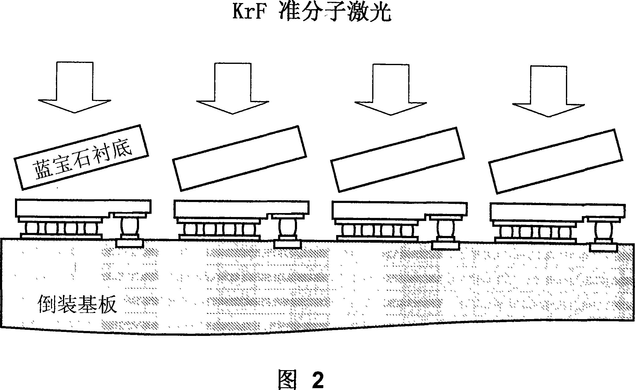
[0048] The present invention will be further described below in conjunction with the accompanying drawings and embodiments.

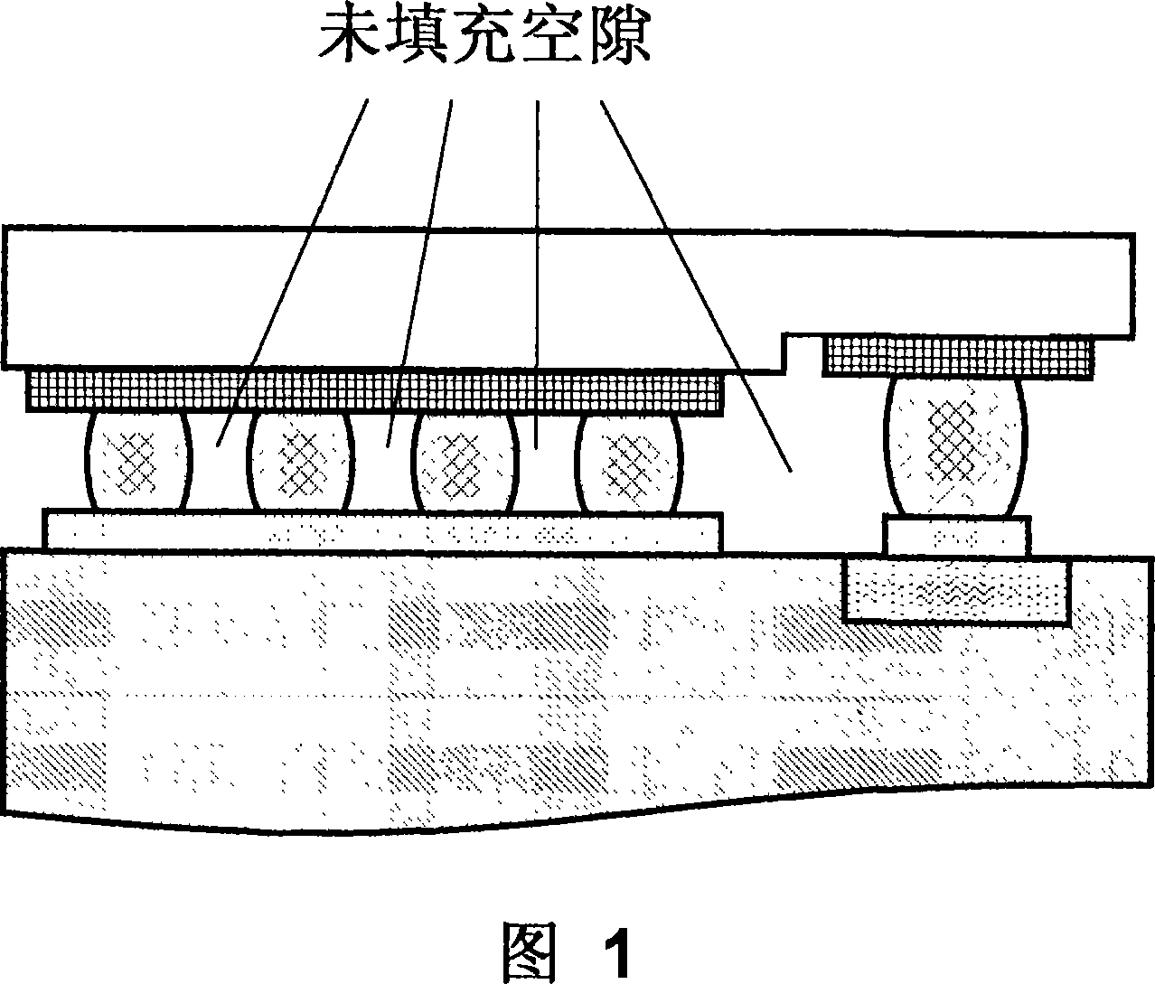
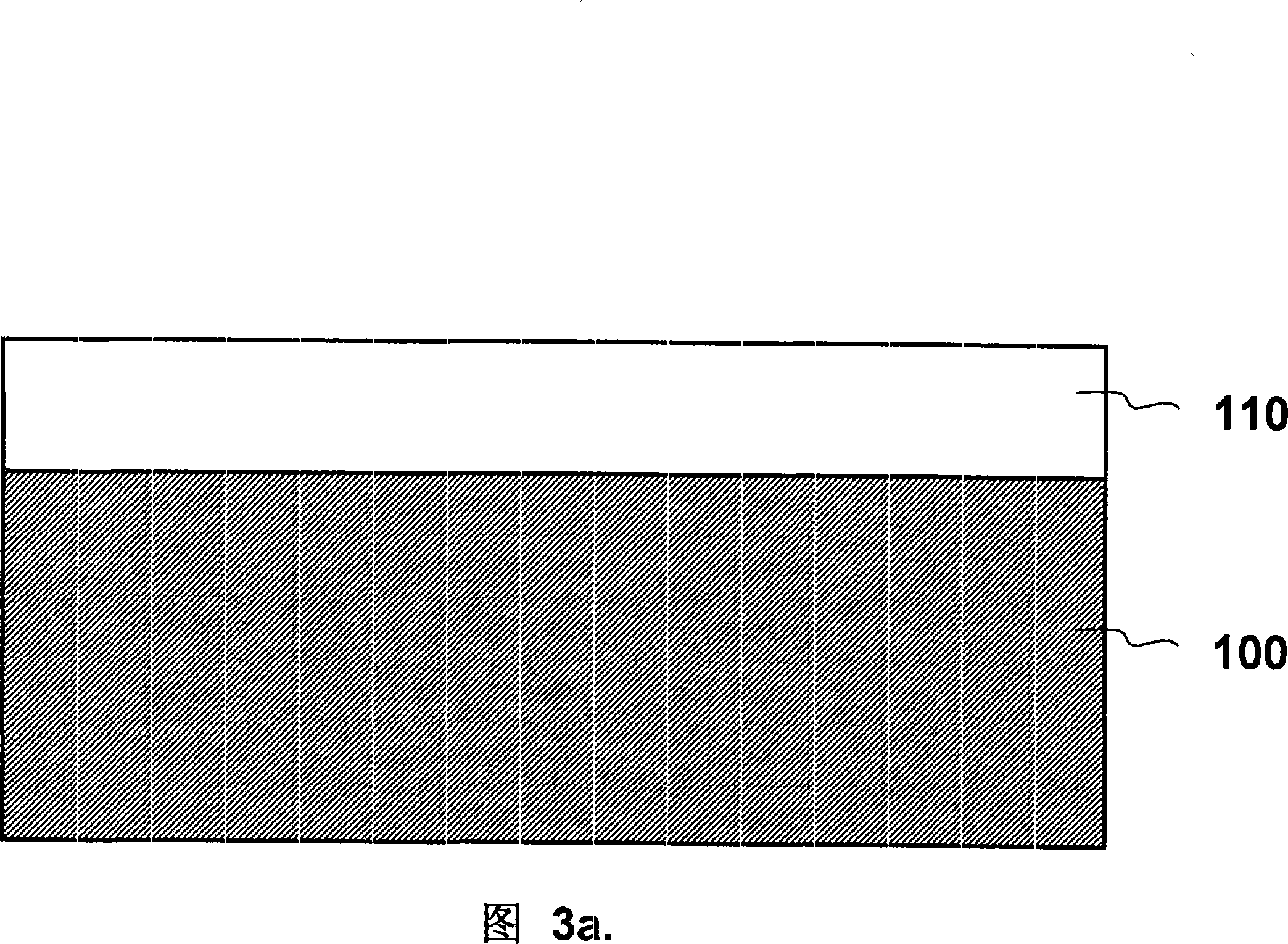
[0049] A kind of thin-film LED chip device based on composite low-resistance buffer structure as shown in Figure 4, its structure is: provide a sapphire substrate 100, grow out to have N semiconductor layer, active layer and P semiconductor layer on the substrate GaN-based epitaxial thin film 110; ohmic contact and metal reflective layer 120 formed on the P semiconductor layer, the material of the reflective metal film is preferably Ag, or one of Al, Ag, Ni, Au, Cu, Pd and Rh metals. An alloy with a thickness between 50 and 500nm; passivation layers 130 and 210 formed in the non-electrical connection area; a multi-metal adhesive layer 150 formed on the reflective metal film; an N electrode formed on the N semiconductor layer. Metal bonding layer 150b; especially form conductive support thick metal layer 160 on multi-metal bonding layer 150, its material...


PUM

PropertyMeasurementUnit
Thicknessaaaaaaaaaa
Diameteraaaaaaaaaa
Thicknessaaaaaaaaaa

Abstract

The present invention provides a film LED chip device basing on the combined low-resistance buffer structure and the manufacturing method thereof, the insulating buffer film is packaged on side wall of all metal structures and is filled in all non-electrical connected areas, with filling in insulating buffer film between all metal convex points which connects the GaN base illuminating device and the electric polarized substrate, the filling-in thickness is a little under or even with the height of the metallic convex points, and with directly liking the GaN base illuminating device crystal disc with the whole surface of the electric polarized inversely mounted substrate with the mode of whole surface linking of the wafer, the metallic convex point of the conductive supporting thick metal layer and the insulating buffer film form the combined low-resistance buffer structure of the invention together, not only the electric connection between the GaN base illuminating device and the electric polarized inversely mounted substrate is realized, but also the buffer layer filling is realized thereby reducing the wafer rupture incidence rate of the subsequent laser stripping technique in order to increase the good product ratio, besides the stripped sapphire substrate disc which can execute finishing to the sapphire substrate and is obtained after stripped operation can be recovered for reusing, the production cost is reduced.

Description

technical field [0001] The invention relates to a light-emitting diode chip, in particular to a thin-film LED chip device based on a composite low-resistance buffer structure and a manufacturing method thereof. Background technique [0002] The existing thin-film LED chip device (TFFC Thin-film Flip Chip) is based on the traditional flip-chip structure chip (FC Flip-Chip size is usually 1mm×1mm), using excimer laser lift-off substrate technology to grow The sapphire (Sapphire) substrate of the GaN material is peeled off, exposing the LED film structure. (Reference 'High performance thin-film flip-chip InGaN-GaN light-emitting diodes' - Philips Lumileds Lighting Company). The problems in the traditional method are as follows: (1) As shown in Figure 1, there is an unfilled gap between the metal bumps used to combine the GaN epitaxial layer film and the flip-chip substrate in the flip-chip structure chip, and the epitaxial layer film is partially lacking. Effective support an...

Claims


Application Information

Patent Timeline
IPC IPC(8): H01L33/00H01L33/12H01L33/40
Inventor 陈文欣潘群峰林雪娇洪灵愿吴志强
Owner XIAMEN SANAN OPTOELECTRONICS TECH CO LTD
Why Eureka
Try Eureka