Method for preparing transistor T type nano grid

A transistor and nanometer technology, which is applied in the field of preparing T-type nano-gates of high electron mobility transistors, can solve the problems of increasing the alignment error of gate caps and gate feet, difficult control of thin line etching, and difficult removal of electron beam glue, etc., to achieve Easy to remove glue, easy to control the development time, easy to produce the effect

Active Publication Date: 2008-10-01
SEMICON MFG INT (SHANGHAI) CORP +1
View PDF0 Cites 3 Cited by
  • Summary
  • Abstract
  • Description
  • Claims
  • Application Information

AI Technical Summary

Problems solved by technology

In this method, after the exposure of the grid cap plate is completed, the epitaxial wafer needs to be taken out of the electron beam lithography machine for development, and then put back into the electron beam lithography machine for the exposure of the grid foot plate, so that moving the sample many times will artificially increase Alignment error of grid cap and grid foot
[0009] In addition, due to the poor adhesion between ZEP520A and the epitaxial wafer, a layer of dielectric needs to be deposited before coating. The dielectric is usually silicon nitride or silicon dioxide. After exposure and development, the dielectric at the gate groove must be etched away. , the etching of nano-sized thin lines is difficult to control, the process is difficult, and the underlying ZEP520A electron beam glue is difficult to remove, which is easy to affect the characteristics of the device

Method used


Image

  • Method for preparing transistor T type nano grid
  • Method for preparing transistor T type nano grid
  • Method for preparing transistor T type nano grid

Examples


Embodiment

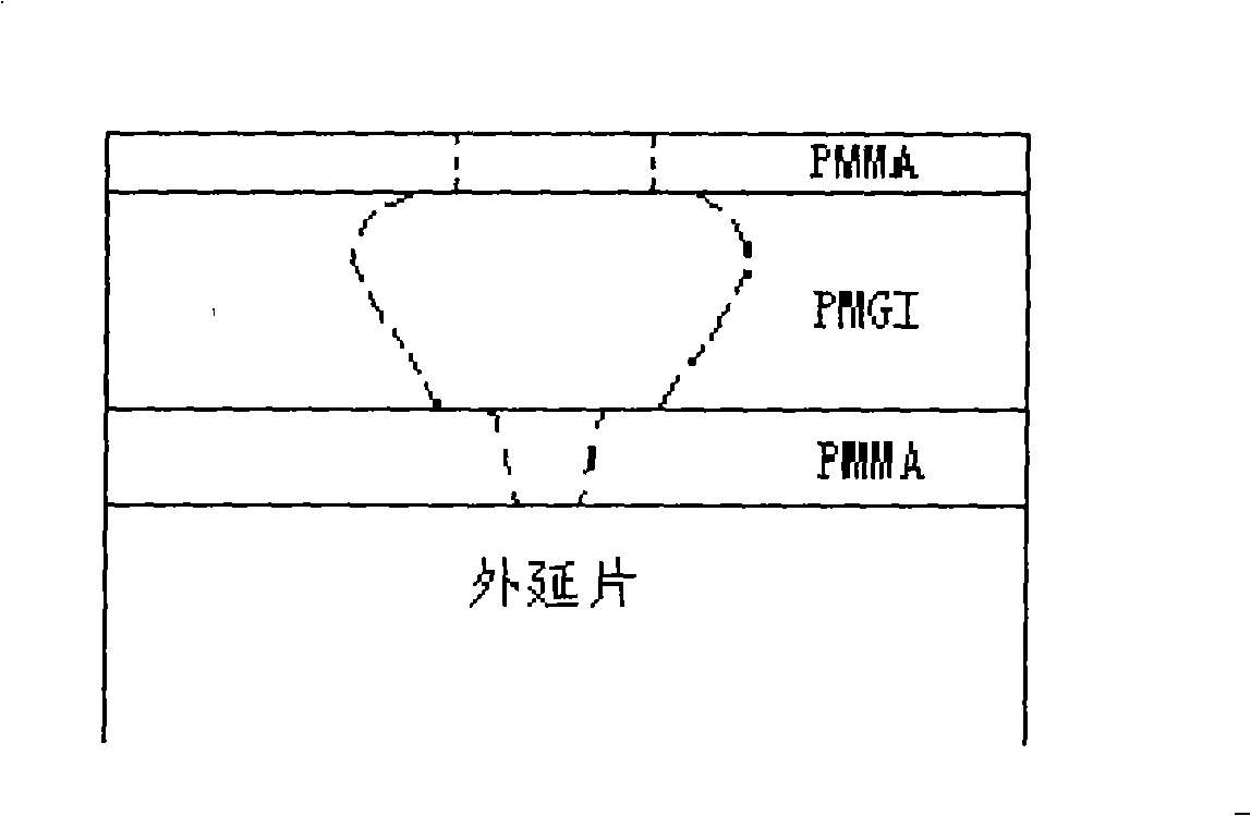
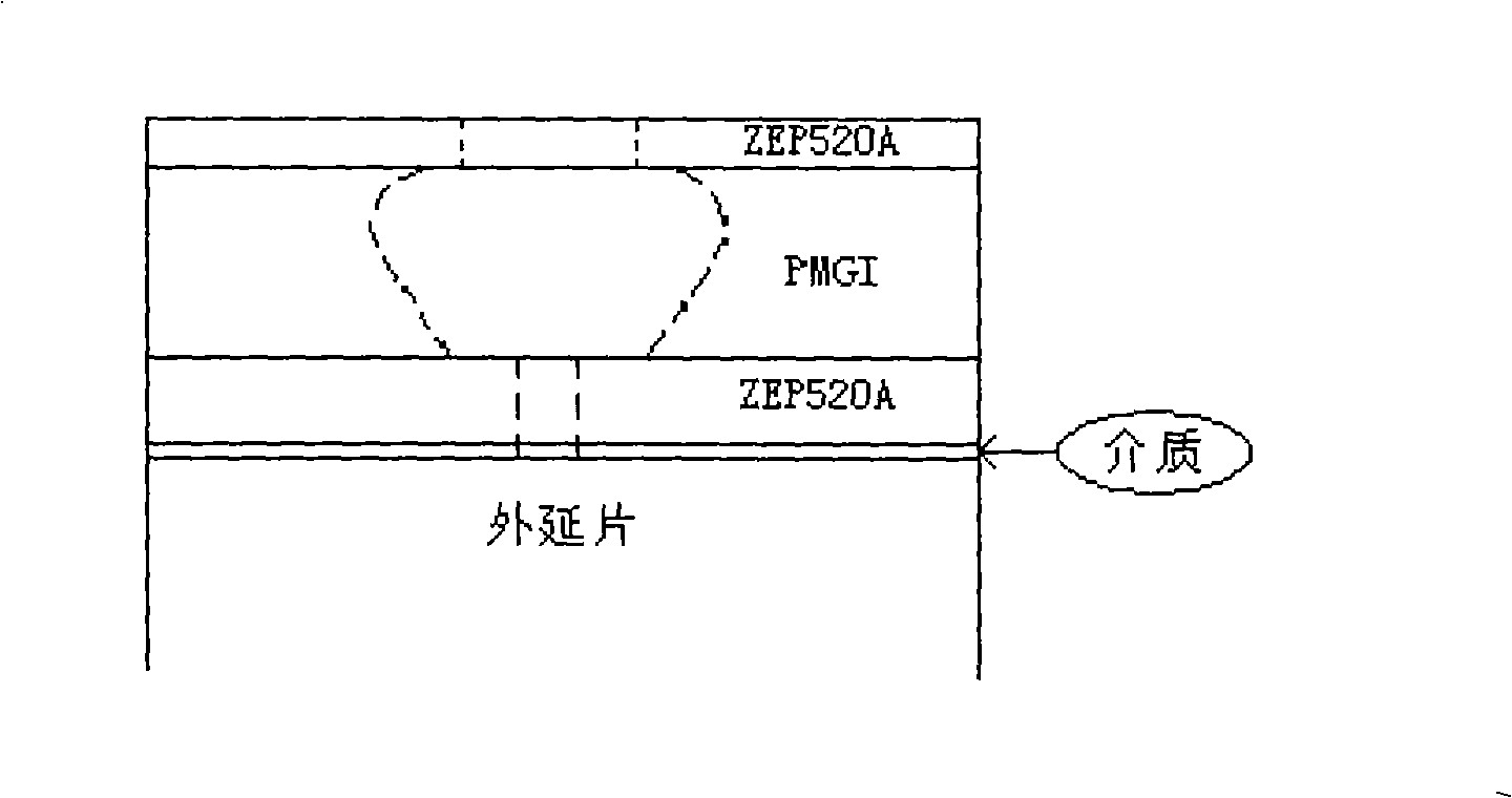
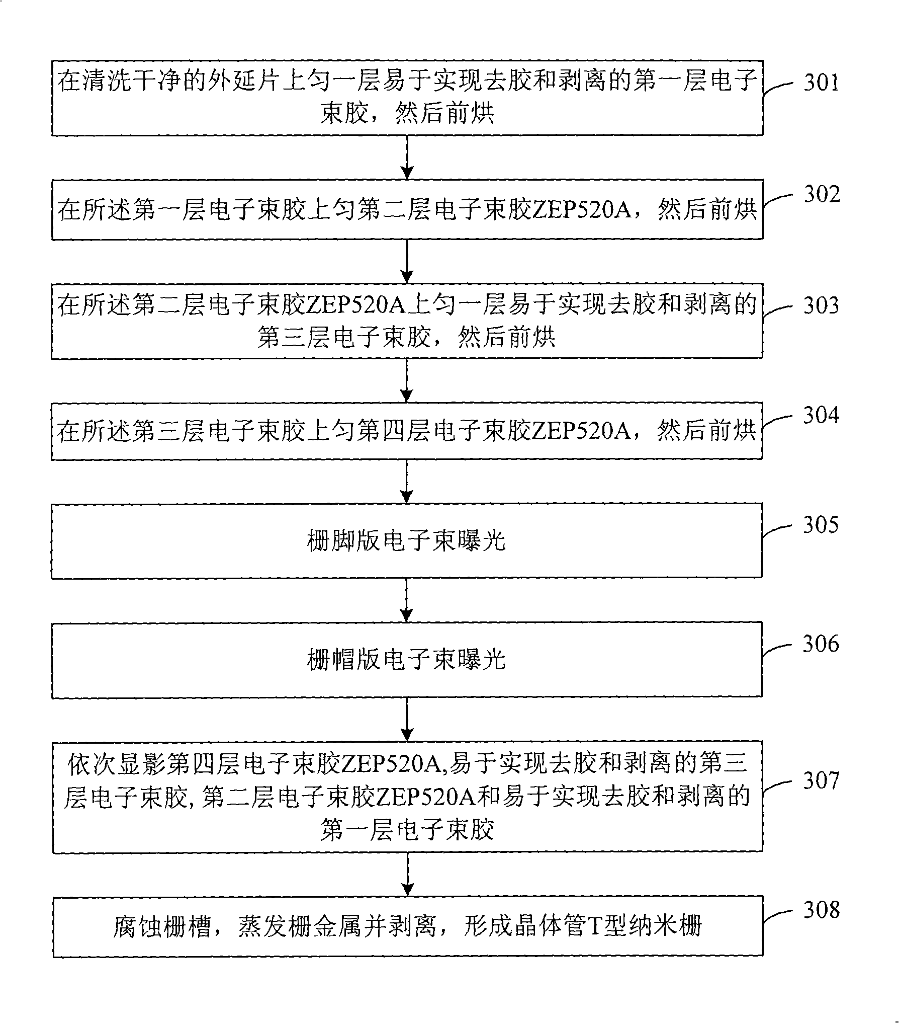
[0071] The method for preparing T-type nano-gates of high electron mobility transistors (HEMT) in this example is to address some shortcomings in the preparation of T-type nano-gates of high electron mobility transistors (HEMTs), using four layers of PMGI / ZEP520A / PMGI / ZEP520A Electron beam photoresist structure (as shown in Table 1) and two electron beam exposure methods to prepare high electron mobility transistor (HEMT) T-type nano-gate.

[0072] Table 1 is a structural representation of the PMGI / ZEP520A / PMGI / ZEP520A four-layer electron beam photoresist used in the method for preparing a high electron mobility transistor (HEMT) T-type nano-gate of the present invention:

[0073]

[0074] Table 1

[0075] In this embodiment, the first layer of electron beam glue and the third layer of electron beam glue that are easy to realize deglue and stripping are PMGI electron beam glue, which is used in the preparation method of high electron mobility transistor (HEMT) T-type nano-g...


PUM


Abstract

The invention discloses a method for manufacturing transistor T-shaped nanometer gate, comprising the steps of: A, coating a first layer electric beam glue which is liable to realize glue-stripping and peeling on a cleaned epitaxial wafer, and then soft-baking; B, coating a second layer electric beam glue ZEP520A on the first layer electric beam glue, and then soft-baking; C, coating a third layer electric beam glue which is liable to realize glue-stripping and peeling on the second layer electric beam glue ZEP520A, and then soft-baking; D, coating a fourth layer electric beam glue ZEP520A on the third layer electric beam glue, and then soft-baking; E, carrying out gate feet electric beam exposure; F, carrying out gate cap electric beam exposure; G, sequentially developing the four layer electric beam glue ZEP520A, the third layer electric beam glue, the second layer electric beam glue ZEP520A and the first layer electric beam glue; H, eroding the gate groove, evaporating and peeling off gate metals to form the transistor T-shaped nanometer gate. Usage of the invention can easily manufacture the gate lines having extremely small size, and the invention has high alignment precision and strong reliability without growth and etching mediums, thus largely reducing the process difficulty.

Description

technical field [0001] The invention relates to the technical field of compound semiconductors, in particular to a method for preparing a T-shaped nano-gate of a high electron mobility transistor. Background technique [0002] Gate preparation is the most critical process in the manufacturing process of High Electron Mobility Transistor (HEMT) devices. Since the gate length directly determines the frequency, noise and other characteristics of the HEMT device, the smaller the gate length, the current cutoff frequency of the device (f T ) and power gain cutoff frequency (f max ) The higher the noise figure of the device is, the smaller the noise figure of the device is. People can obtain devices with better characteristics by continuously reducing the gate length of high electron mobility transistor (HEMT) devices. [0003] As the gate length shortens, the gate resistance increases, and when the gate length decreases below 0.5 μm, the microwave loss of the gate resistance ma...

Claims


Application Information

Patent Timeline
Patent Type & Authority Applications(China)
IPC IPC(8): H01L21/28H01L21/335
Inventor 刘亮张海英刘训春
Owner SEMICON MFG INT (SHANGHAI) CORP
Why Eureka
Try Eureka