
Photoelectric device based on carbon nano-tube, optoelectronic integrated circuit unit and circuit

A technology of carbon nanotubes and integrated circuits, applied in the field of nanoelectronics, can solve problems affecting silicon-based optoelectronic devices, scale differences are unlikely, and integrate together to achieve the effect of a simple device structure

Inactive Publication Date: 2008-10-08
PEKING UNIV
View PDF2 Cites 20 Cited by
  • Summary
  • Abstract
  • Description
  • Claims
  • Application Information

AI Technical Summary

Problems solved by technology

Another more serious defect of silicon-based materials is that silicon is not a direct bandgap semiconductor. This defect has seriously affected the development of silicon-based optoelectronic devices, resulting in silicon-based integrated circuits and semiconductor optoelectronic devices basically following two parallel paths. actual state of development
Although there have been important breakthroughs in the development of silicon-based optoelectronic devices in recent years, the difference in scale between silicon-based optoelectronic devices and CMOS devices makes it impossible to integrate the two organically in the near future

Method used


Image

  • Photoelectric device based on carbon nano-tube, optoelectronic integrated circuit unit and circuit
  • Photoelectric device based on carbon nano-tube, optoelectronic integrated circuit unit and circuit
  • Photoelectric device based on carbon nano-tube, optoelectronic integrated circuit unit and circuit

Examples


Embodiment 1

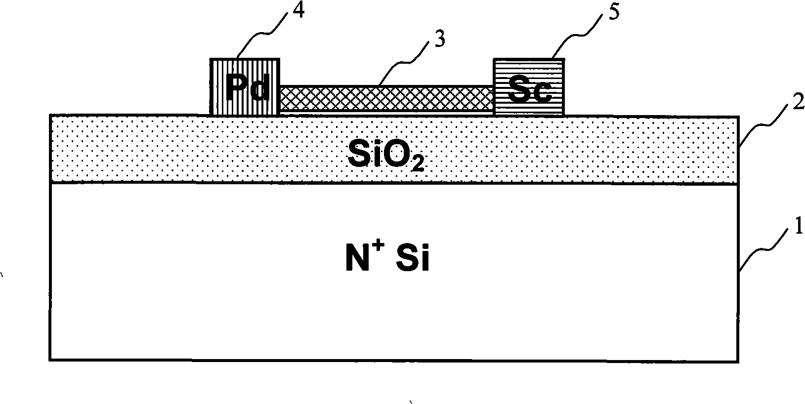
[0048] The structure of the single-walled carbon nanotube high-performance multifunctional optoelectronic device with Pd and Sc as the source and drain electrodes is as follows: figure 1 As shown, including a conductive substrate 1, a SiO 2 An insulating layer 2 and a carbon nanotube 3, and the carbon nanotube 3 has a Pd electrode 4 and a Sc electrode 5 in direct contact with it. Concrete preparation steps are as follows:

[0049] 1. By positioning growth, or dropping the dispersed single-walled carbon nanotube solution onto the marked Si / SiO 2 on the substrate, thus obtaining the Si / SiO 2 A single-walled carbon nanotube on a substrate;

[0050] 2. Observing with a scanning electron microscope or an atomic force microscope, record the specific position of the single-walled carbon nanotubes;

[0051] 3. Apply photoresist on the substrate and form the shape of the Pd electrode by optical exposure or electron beam lithography;

[0052] 4. Put the photolithographic sample int...

Embodiment 2

[0058] The structure of the basic unit of the large-scale optoelectronic integrated circuit based on carbon nanotubes with the top gate structure is shown in Figure 11, including a conductive substrate 1, a SiO 2 An insulating layer 2, a carbon nanotube 3, and two Pd electrodes 4 and two Sc electrodes 5 arranged sequentially on the carbon nanotube 3, and the carbon nanotubes between each Pd electrode and Sc electrode are covered with a grid dielectric layer 6. On the gate dielectric layer is the top gate electrode 7 . Concrete preparation process comprises the following steps:

[0059] 1. By positioning growth, or dropping the dispersed carbon nanotube solution onto the marked Si / SiO 2 on the substrate, obtained on Si / SiO 2 One or more parallel carbon nanotubes on a substrate;

[0060] 2. Observe and record the specific position of carbon nanotubes through scanning electron microscope or atomic force microscope;

[0061] 3. Apply photoresist on the substrate and form the s...

Embodiment 3

[0070] A large-scale optoelectronic integrated circuit based on carbon nanotubes such as Figure 14 As shown, two parallel carbon nanotubes 3 are located on the conductive substrate 1 and the insulating layer 2 , and a plurality of Pd electrodes 4 and a plurality of Sc electrodes 5 are arranged on the carbon nanotubes 3 . Its specific preparation process comprises the following steps:

[0071] 1. By positioning growth, or dropping the dispersed carbon nanotube solution onto the marked Si / SiO 2 on the substrate, obtained on Si / SiO 2 One or more parallel carbon nanotubes on a substrate;

[0072] 2. Observe and record the specific position of carbon nanotubes through scanning electron microscope or atomic force microscope;

[0073] 3. Apply photoresist and form all the Pd electrode shapes required in the figure by optical exposure or electron beam lithography;

[0074] 4. Put the photolithographic sample into the electron beam evaporation system, and evaporate a layer of meta...


PUM


Abstract

The invention provides a photoelectric device based on carbon nano-tube, which uses carbon nano-tube as conductive channel. One end of the photoelectric device has a high work function metal electrode, the other end of the photoelectric device has a low work function metal electrode, the photoelectric device can realize various functional device by simple structure and includes but is not limited to anambipolar field effect transistor, a non-resistance ambipolar diode, a luminescent diode and an optical detector. The invention also provides a large-scale photoelectricity integrated circuit basic unit based on the carbon nano-tube, which uses carbon nano-tube as conductive channel. Two high work function metal electrodes and two low work function metal electrodes are sequentially arranged on the carbon nano-tube, various functional device including electronic device and photoelectric device can be obtained by agilely setting voltage of each electrode. The invention further provides a large-scale photoelectricity integrated circuit capable of realizing various function. In the present invention, function of existing integrated circuit chip is hopeful to greatly increase, novel design thoughts and effective application method can be provided to scale integrated nano circuit.

Description

technical field [0001] The invention belongs to the field of nanoelectronics, in particular to a high-performance multifunctional photoelectric device based on carbon nanotubes, a basic unit of a large-scale photoelectric integrated circuit and an photoelectric integrated circuit. Background technique [0002] After more than 40 years of rapid development, the development of silicon-based CMOS transistors has become perfect, and the corresponding CMOS devices are reaching their physical limits. The current mainstream 45nm technology has adopted high-k technology and metal gates to replace SiO 2 The gate insulating layer and highly doped polysilicon electrodes, the most important silicon conduction channel in the device, are gradually being replaced by stressed silicon. Although the development of 32nm technology is coming to an end, there is still no mature plan on how to develop microelectronics after 32nm technology. In Intel's transistor development roadmap, carbon nano...

Claims


Application Information

Patent Timeline
Patent Type & Authority Applications(China)
IPC IPC(8): H01L31/10H01L31/11H01L33/00H01L27/02H01L27/144H01L27/15H01L33/34
CPCH01L27/15B82Y10/00H01L33/34H01L51/0048H01L51/0545H01L51/105H10K85/221H10K10/84H10K10/466
Inventor 彭练矛梁学磊张志勇王胜陈清
Owner PEKING UNIV
Learn More