Aligning mark used for photolithography equipment aligning system and its use method

A technology for aligning marks and aligning systems, applied in the direction of microlithography exposure equipment, optics, photoplate making process of pattern surface, etc. The assembly and adjustment requirements are very high, so as to improve the alignment signal strength and the dynamic range of detection, reduce the alignment position error, and improve the energy utilization rate.

Active Publication Date: 2008-11-05
SHANGHAI MICRO ELECTRONICS EQUIP (GRP) CO LTD +1
View PDF2 Cites 26 Cited by
  • Summary
  • Abstract
  • Description
  • Claims
  • Application Information

AI Technical Summary

Problems solved by technology

However, when using a wedge array, the requirements for the surface shape and wedge angle consistency of the two wedges with the same positive and negative orders of refraction are very high; and the requirements for the manufacturing, assembly and adjustment of the wedge plate group are also very high. It is difficult and expensive to realize the project
[0008] Another prior art situation (see (2) Chinese invention patent, publication number: 200710044152.1, title of invention: an alignment system for lithography equipment), the alignment system uses a three-period phase The grating only uses the first-order diffracted light of these three periods as the alignment signal, which can achieve a large capture range and high alignment accuracy, and only uses the first-order diffracted light of each period to obtain a stronger signal strength , improve the signal-to-noise ratio of the system, and do not need to use adjustment devices such as wedges to separate multi-channel high-order diffraction components, simplifying the optical path design and debugging difficulty, but the alignment marks in the alignment system are lined up on the silicon wafer and the reference board distribution, which reduces the utilization rate of the light source, and this arrangement mode scans the corresponding reference grating when each group of grating images of the alignment mark scans the corresponding reference grating, and the grating images of different periods scan a reference grating at the same time, which will cause the scanning signal. Crosstalk problem, which is not conducive to the alignment of lithography equipment

Method used


Image

  • Aligning mark used for photolithography equipment aligning system and its use method
  • Aligning mark used for photolithography equipment aligning system and its use method
  • Aligning mark used for photolithography equipment aligning system and its use method

Examples


Embodiment Construction

[0039] The specific embodiments of the present invention will be further described below with reference to the accompanying drawings.

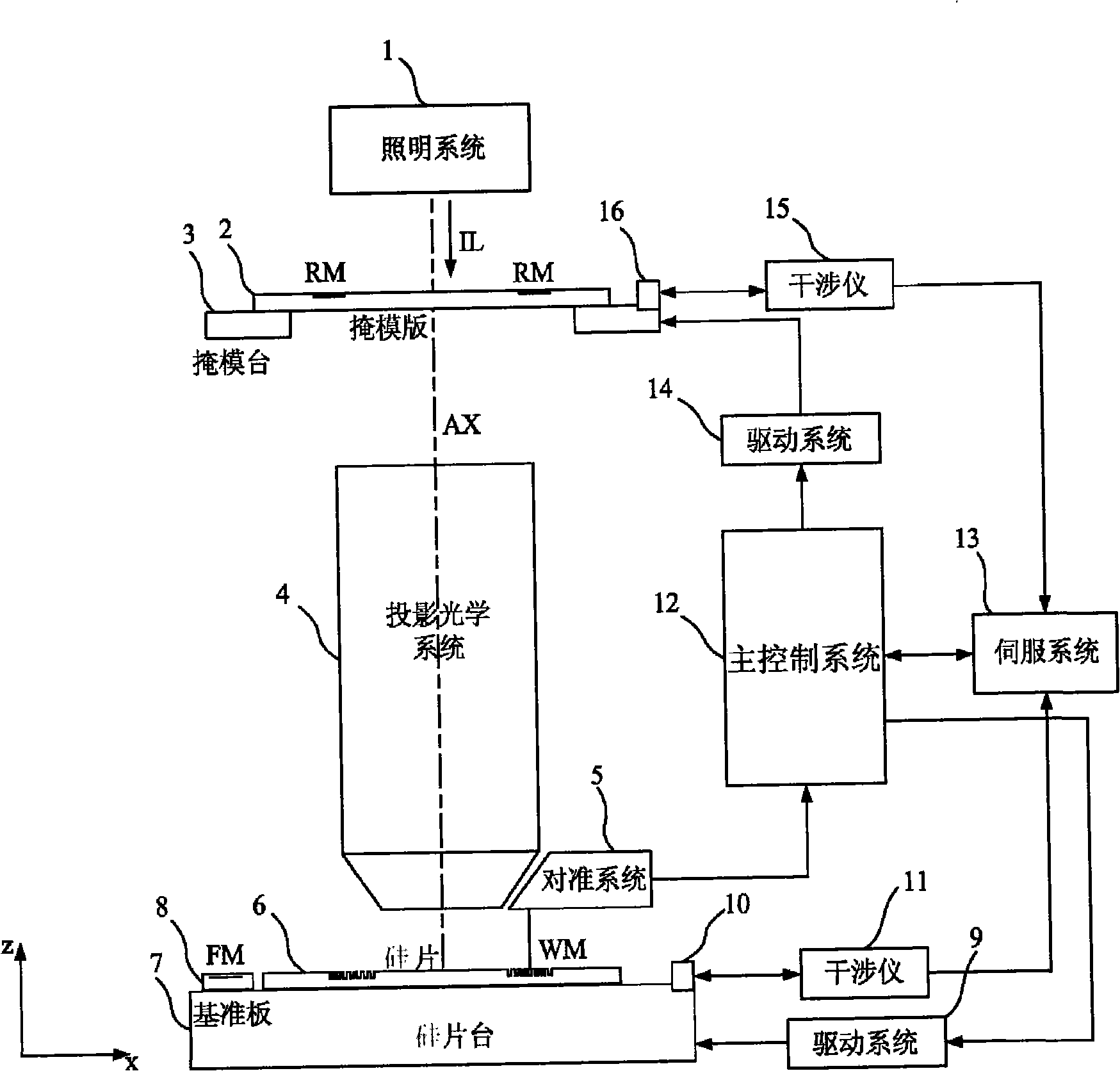
[0040] figure 1 The general layout and working principle structure diagram between the alignment system of the lithography apparatus used in the present invention and the lithography apparatus are shown. The composition of the lithography apparatus includes: an illumination system 1 for providing an exposure beam; a mask holder and a mask stage 3 for supporting a reticle 2, and the reticle 2 has a mask pattern and an alignment mark with a periodic structure RM; projection optical system 4 for projecting the mask pattern on the reticle 2 to the silicon wafer 6; a silicon wafer holder and a silicon wafer stage 7 for supporting the silicon wafer 6, and the silicon wafer stage 7 is engraved with fiducial marks FM reference plate 8, alignment marks with periodic optical structures on silicon wafer 6; off-axis alignment system 5 for mask and wafer ...


PUM


Abstract

The present invention provides an aligning mark which is used for the aligning system of the photo-etching device and a using method thereof. The aligning mark comprising at least three groups of raster with different periods is used. The + / -1 grade diffraction lights of three groups of raster are used in the aligning process. Two large-period raster in three groups of raster are used for coarse alignment. A small-period raster is used for refined alignment. The alignment position error caused by the asymmetrical deformation of the aligning mark is reduced. The small period raster and the large period raster are spatially staggered. The corresponding interface images are spatially divided in the image surface. The crosstalk problem of signal is effectively settled. The energy usage of light source is increased. The intensity of aligning signal and the dynamic range of detection are facilitated to increase.

Description

technical field [0001] The present invention relates to a lithography apparatus in the field of integrated circuit or other micro device manufacturing, and in particular to an alignment mark of an alignment system. Background technique [0002] The lithography equipment in the prior art is mainly used for the manufacture of integrated circuits IC or other micro devices. Through a lithographic apparatus, multiple layers of masks with different mask patterns are sequentially exposed and imaged on a photoresist-coated silicon wafer with precise alignment. The current lithography equipment is generally divided into two categories, one is the stepper lithography equipment, the mask pattern is imaged on one exposure area of ​​the silicon wafer at one time, and then the silicon wafer moves relative to the mask to move the next exposure area Go under the mask pattern and the projection objective, and once again expose the mask pattern to another exposed area of ​​the silicon wafer,...

Claims


Application Information

Patent Timeline
Patent Type & Authority Applications(China)
IPC IPC(8): G03F7/20G03F9/00
Inventor 杜聚有徐荣伟戈亚萍
Owner SHANGHAI MICRO ELECTRONICS EQUIP (GRP) CO LTD
Why Eureka
Try Eureka