Gallium nitride thin film epitaxial growth structure and method

A technology of epitaxial growth and gallium nitride, which is applied in the structure and field of epitaxial growth of gallium nitride thin films, can solve the problems of large mismatch stress, achieve the effects of improving crystal quality, reducing dislocation density, and simple process

Active Publication Date: 2008-11-12
NO 55 INST CHINA ELECTRONIC SCI & TECHNOLOGYGROUP CO LTD
View PDF0 Cites 18 Cited by
  • Summary
  • Abstract
  • Description
  • Claims
  • Application Information

AI Technical Summary

Problems solved by technology

However, since there is still a large mismatch stress between the top silicon of SOI and the epitaxially grown GaN single crystal film, it is necessary to further explore effective methods to reduce stress and improve film quality

Method used


Image

  • Gallium nitride thin film epitaxial growth structure and method

Examples


Embodiment 1

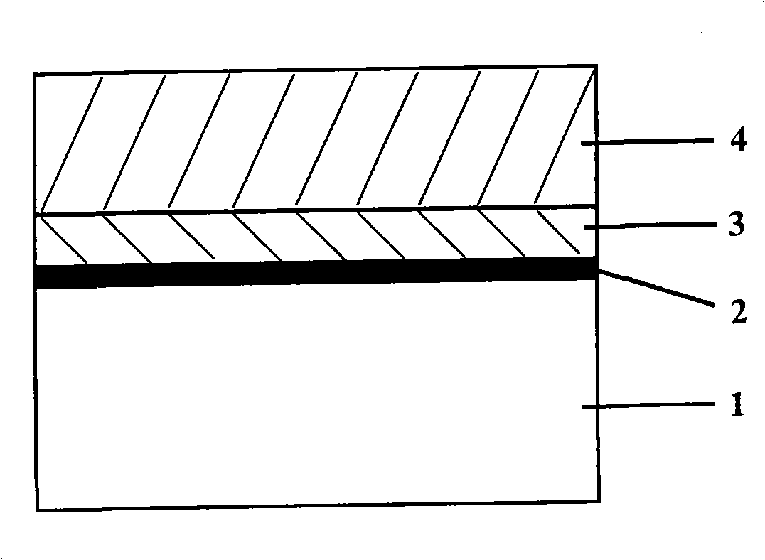
[0024] 1) Select the SOI substrate and load it into the MOCVD reaction chamber;

[0025] 2) Bake at 1150°C, 100Torr, hydrogen atmosphere (10L / min) for 10 minutes;

[0026] 3) Raise the temperature to 1180°C, pass through trimethylaluminum (30mL / min) for 30 seconds, then pass through ammonia gas (3000mL / min) and trimethylaluminum (30mL / min) to grow a 60nm thick AlN nucleation layer;

[0027] 4) Turn off trimethylaluminum, feed ammonia gas (1520mL / min) and trimethylgallium (85μmol / min), V / III ratio is 800, and grow a 1.0μm thick GaN buffer layer;

[0028] 5) Cool down to 1040°C, inject ammonia gas (4400mL / min) and trimethylgallium (130μmol / min), and grow a 2.0μm thick GaN film;

[0029] 6) Reduce to room temperature.

Embodiment 2

[0031] 1) Select the SOI substrate and load it into the MOCVD reaction chamber;

[0032] 2) Bake at 1150°C, 100Torr, hydrogen atmosphere (10L / min) for 10 minutes;

[0033] 3) Cool down to 1040°C, pass through trimethylaluminum (30mL / min) for 30 seconds, then pass through ammonia gas (3000mL / min) and trimethylaluminum (30mL / min) to grow a 60nm thick AlN nucleation layer;

[0034] 4) Turn off the trimethylaluminum, lower the temperature to 800°C, feed ammonia gas (1366mL / min) and trimethylgallium (305μmol / min), the V / III ratio is 200, and grow a 0.5μm thick GaN buffer layer;

[0035] 5) Raise the temperature to 1040°C, inject ammonia gas (4400mL / min) and trimethylgallium (130μmol / min), and grow a 2.0μm thick GaN single crystal film;

[0036] 6) Reduce to room temperature.

Embodiment 3

[0038] 1) Select the SOI substrate and load it into the MOCVD reaction chamber;

[0039] 2) Bake at 1150°C, 100Torr, hydrogen atmosphere (10L / min) for 10 minutes;

[0040] 3) Cool down to 1040°C, pass through trimethylaluminum (30mL / min) for 30 seconds, then pass through ammonia gas (3000mL / min) and trimethylaluminum (30mL / min) to grow a 60nm thick AlN nucleation layer;

[0041] 4) Turn off the trimethylaluminum, lower the temperature to 980°C, feed ammonia gas (1702mL / min) and trimethylgallium (152μmol / min), the V / III ratio is 500, and grow a GaN buffer layer with a thickness of 0.1μm;

[0042] 5) Raise the temperature to 1040°C, inject ammonia gas (4400mL / min) and trimethylgallium (130μmol / min), and grow a 2.0μm thick GaN single crystal film;

[0043] 6) Reduce to room temperature.


PUM


Abstract

The invention relates to a gallium nitride membrane epitaxial growth structure and a method. The structure is as follows: an SOI substrate is provided with an AIN nucleation layer which is provided with a low V / III ratio GaN cushioning layer; and the low V low V / III ratio / III ratio cushioning layer is provided with a GaN single-crystal membrane. The method is as follows: the SOI substrate is selected and arranged inside an MOCVD reaction chamber; the SOI substrate is roasted and cooled down, and then trimethyl aluminum is added to the SOI substrate so as to grow the AIN nucleation layer; the trimethyl aluminum is closed and cooled down, and then ammonia gas is injected to the rimethyl aluminum so as to grow the GaN cushioning layer; the GaN cushioning layer is heated up and injected with ammonia gas and trimethyl gallium so as to grow the GaN single-crystal membrane; finally, the temperature is cooled down to room temperature. The gallium nitride membrane epitaxial growth structure and the method have the advantages that: when the low V / III ratio GaN cushioning layer is converted into quasi-two-dimensional growth from three-dimensional growth with prolonging a GaN membrane, crystal grain is fully grown up so as to reduce crystal grain density, release mismatch stress and increase the mass of a GaN membrane crystal; moreover, the mismatch stress of the SOI substrate GaN single-crystal membrane is reduced by means of the low V / III ratio GaN cushioning layer, thereby reducing dislocation density and increasing crystal quality.

Description

technical field [0001] The invention relates to an epitaxial growth structure and method of a semiconductor single crystal thin film, in particular to a gallium nitride (GaN) buffer layer with a low V / III ratio (the molar ratio of group V elements to group III elements) to improve the insulator The structure and method of GaN epitaxial thin film quality on silicon-on-insulator (SOI: Silicon-on-Insulator) substrate. Background technique [0002] At present, due to factors such as manufacturing costs, the epitaxial growth of gallium nitride (GaN) single crystal thin films on silicon (Si) substrates has become a research hotspot. Si substrate has unique advantages such as low price, large size, high crystal quality, good thermal conductivity, low hardness, and easy processing. Therefore, Si-based GaN epitaxial growth technology is considered to be an industrialized technology with low cost and broad market prospects. [0003] Due to the large mismatch (lattice and thermal) be...

Claims


Application Information

Patent Timeline
Patent Type & Authority Applications(China)
IPC IPC(8): C30B29/38C30B25/02C30B25/18
Inventor 李忠辉陈辰董逊
Owner NO 55 INST CHINA ELECTRONIC SCI & TECHNOLOGYGROUP CO LTD
Why Eureka
Try Eureka